Graphene and Dirac Materials
Graphene is a single atomic layer of carbon whose low-energy bands meet at two inequivalent valleys and realize two-dimensional Dirac quasiparticles. The Dirac structure is emergent: the microscopic electrons are nonrelativistic, while a two-component sublattice amplitude obeys a first-order continuum Hamiltonian near each band touching.
The phrase Dirac material is broader than graphene. It denotes a solid whose low-energy bands contain approximately linear crossings described by a Dirac-like Hamiltonian over a controlled momentum and energy window. The Pauli matrices may represent sublattice, orbital, layer, or real-spin mixtures; the crossing may be two- or three-dimensional; and its stability depends on lattice symmetry, topology, or tuning. A cone-shaped dispersion by itself does not identify those ingredients.
This page owns graphene as a material and diagnostic platform: honeycomb and valley bookkeeping, pseudospin, the physical meaning of its Berry phase, the Dirac Landau ladder, realistic corrections, and the bridge from monolayer cones to moiré minibands. Landau Levels in Solids owns the controlled comparison between this Dirac ladder and parabolic or nonparabolic material-band ladders; it does not replace graphene’s sublattice, valley, or zero-mode derivation here. Tight-Binding Models owns the general localized-orbital method. Graphene Dirac Model is the compact convention card. Berry Phase owns the general geometric construction. The later moiré chapter owns continuum-model construction, flat bands, correlated phases, and platform comparisons.
Honeycomb Crystal
Section titled “Honeycomb Crystal”Graphene’s carbon atoms form a planar honeycomb network. Three in-plane bonds per atom build strong bands. The remaining orbital contributes to the low-energy and bands.
The honeycomb is not a Bravais lattice. It is a triangular Bravais lattice with two sites, conventionally and , in each primitive cell. Translation symmetry therefore produces a two-component Bloch amplitude
Keeping one orbital per site and nearest-neighbor hopping gives
where join one site to its three neighbors. The bands are
At two inequivalent Brillouin-zone corners, denoted and , the three phase factors cancel:
The band touching is therefore an interference result tied to the two-site basis and crystal symmetries, not a generic property of every hexagonal drawing.
Symmetries of the minimal model
Section titled “Symmetries of the minimal model”With only hopping between opposite sublattices,
This sublattice, or chiral, symmetry pairs energies at . Real graphene has same-sublattice hopping and other corrections that break exact particle–hole symmetry without necessarily opening a gap. Conversely, a sublattice potential
opens a gap because it distinguishes from .
Time reversal interchanges and . Smooth scalar disorder transfers little crystal momentum and approximately preserves the valley label, whereas atomic defects, armchair edges, and short-range potentials can mix valleys. Valley is thus a useful low-energy quantum number, not an inviolable microscopic conservation law.
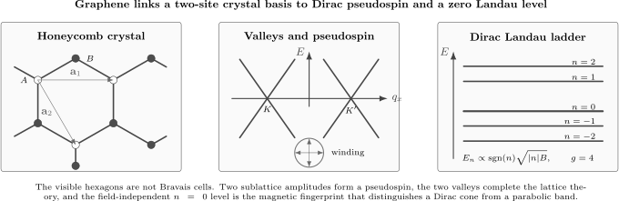
The honeycomb crystal has a triangular Bravais lattice and an basis. Expanding its two-band Bloch Hamiltonian near and produces sublattice-pseudospin Dirac cones. A perpendicular magnetic field yields levels proportional to , including the characteristic level.
Dirac Cones
Section titled “Dirac Cones”Write
where labels the two valleys. In one common basis and orientation, the leading continuum Hamiltonian is
The Pauli matrices act on sublattice amplitudes. Real spin supplies an additional near-degeneracy in the minimal model. The spectrum is
with for the conduction band and for the valence band. A representative graphene velocity is
about three hundred times smaller than the speed of light. It is a band velocity set mainly by hopping and bond length, not a new fundamental limiting speed.
The continuum expansion is controlled only when
and the energy remains well below the lattice bandwidth. It cannot be extended to the entire Brillouin zone, used to count only one valley, or regulated without restoring the lattice’s ultraviolet information.
Density, DOS, and cyclotron mass
Section titled “Density, DOS, and cyclotron mass”Including spin and valley gives ideal degeneracy . For a circular Fermi contour,
so
The sign of distinguishes electron and hole doping. The ideal density of states per area is
It vanishes linearly at charge neutrality rather than remaining constant as in a parabolic 2DEG. The quantum capacitance per area is
Graphene has no constant curvature mass at the cone. A semiclassical cyclotron orbit at energy instead has
Effective Mass owns why this orbit mass is meaningful even when a band-edge curvature mass is not.
Charge neutrality is not an empty vacuum
Section titled “Charge neutrality is not an empty vacuum”At ideal neutrality, valence states are filled and conduction states are empty up to the touching. In a device, trapped charge and disorder commonly create electron–hole puddles with a residual density scale . Contacts, strain, substrate potential, finite temperature, and interaction corrections can all broaden the neutrality region.
Consequently, a finite “minimum conductivity” is not a universal number determined by the clean Dirac Hamiltonian alone. Its measured value depends on aspect ratio, contacts, disorder class, inhomogeneity, and order of limits. Two-Dimensional Electron Gases supplies the transport-versus-quantum-lifetime and multiband-density warnings, but a constant-mass Drude formula must be translated to graphene’s energy-dependent kinematics.
Sublattice Pseudospin
Section titled “Sublattice Pseudospin”Let
A normalized eigenstate in the chosen convention can be written
Its pseudospin expectation is
The pseudospin winds once as momentum encircles a valley. This momentum–pseudospin locking is often called chirality in graphene. It is not real-spin helicity, although real spin can become coupled through spin–orbit interactions.
Backscattering overlap
Section titled “Backscattering overlap”For scalar disorder that acts equally on and and does not change valley, the same-band overlap is
Exact intravalley backscattering has and vanishes in this minimal model. This does not make graphene immune to resistance. Intervalley scattering, sublattice-asymmetric disorder, ripples, phonons, edges, multiple scattering, contacts, and interaction effects all relax current.
The same spinor matching gives high transmission near normal incidence through a sufficiently smooth electrostatic – junction, commonly called Klein tunneling. Perfect transmission is tied to ideal chirality, smoothness, incidence angle, and the absence of a relevant mass or intervalley term. It is not a statement that every graphene barrier is transparent.
Berry Phase
Section titled “Berry Phase”As a state moves around one valley, the pseudospin follows the in-plane momentum texture. The geometric phase around a loop enclosing one ideal cone is
The orientation and valley set the sign, while and are equivalent modulo . A loop enclosing both valleys has the lattice-completed phase content, and the two valley contributions cannot be discarded when computing global invariants.
In semiclassical orbit quantization,
For , the usual one-half offset is canceled. This shift underlies the zero Landau level and the phase of ideal quantum oscillations.
What the π phase does not prove
Section titled “What the π phase does not prove”A measured Landau-fan intercept is not automatically a precision Berry-phase measurement. Zeeman splitting, multiple frequencies, three-dimensional curvature, density drift, field-dependent chemical potential, disorder, and an arbitrary indexing convention can shift the fitted intercept. A credible inference reports the indexing rule, fit window, uncertainty, degeneracy, and complementary band information.
Nor does a Berry phase alone make gapless graphene a two-dimensional topological insulator. The massless cone has a singular gauge structure at the touching, but the full time-reversal-symmetric lattice has two valleys and zero net charge Chern number.
Adding a mass,
tilts the pseudospin out of plane and changes the loop phase continuously with Fermi energy. For an ideal circular conduction-band orbit, its magnitude has the form
with valley- and orientation-dependent sign. A simple sublattice mass produces opposite valley Berry curvature and zero total Chern number. A Haldane-type valley-dependent mass can make the valley contributions add, but the full lattice model, not one isolated cone, determines the integer invariant.
Landau Levels
Section titled “Landau Levels”Apply a perpendicular magnetic field through minimal coupling,
for an electron of charge . The Dirac Hamiltonian couples the two sublattice components through harmonic-oscillator ladder operators. The monolayer spectrum is
Unlike parabolic levels, the spacing is not constant and scales as . The level remains at the Dirac-point energy in the ideal particle–hole-symmetric model.
For one sign of , the zero-mode envelope at occupies one sublattice and the zero mode at occupies the other; reversing the field reverses the assignment. This valley–sublattice structure is one reason mass terms and interactions act unusually within the zero level.
Each unresolved orbital level has spin–valley multiplicity four and degeneracy per area
The ideal monolayer Hall sequence is
The “half integer” refers to the offset per flavor; the measured total Hall conductivity remains an integer multiple of . Zeeman coupling, interactions, substrate alignment, strain, or valley anisotropy can split the fourfold multiplet and produce additional integer plateaus.
The canonical plateau mechanism, localization, edge channels, and resistance metrology live at Integer Quantum Hall Effect. Interaction-driven fractions and symmetry-broken graphene states live within the broader framework at Fractional Quantum Hall Effect.
Magnetic and optical fingerprints
Section titled “Magnetic and optical fingerprints”The Dirac ladder can be tested several ways:
- scanning tunneling spectroscopy resolves levels with scaling;
- Shubnikov–de Haas oscillations test frequency, degeneracy, and phase;
- Hall plateaus test the zero-level offset and resolved symmetry breaking;
- infrared transitions approximately obey in the clean dipole model;
- quantum capacitance resolves the DOS peaks thermodynamically.
Agreement among these probes is stronger than fitting one fan diagram.
Beyond the Minimal Cone
Section titled “Beyond the Minimal Cone”The nearest-neighbor, noninteracting, free-standing model is a starting point. Real graphene includes:
| Correction | Leading effect | Diagnostic |
|---|---|---|
| next-neighbor hopping | particle–hole asymmetry | asymmetric electron and hole dispersion |
| trigonal warping | noncircular contours away from neutrality | angle-resolved dispersion and orbit shape |
| strain | anisotropic velocities and valley-dependent pseudogauge fields | Raman maps, local spectroscopy, transport anisotropy |
| substrate or aligned hBN | dielectric screening, disorder reduction, possible sublattice mass, moiré potential | gap, secondary neutrality points, Hofstadter spectrum |
| charged disorder | puddles and density-dependent mobility | scanning probes, gate dependence, noise |
| short-range defects and edges | intervalley scattering | Raman peak, weak localization, edge dependence |
| electron interactions | velocity renormalization and broken-symmetry states | density-dependent spectroscopy and thermodynamics |
| spin–orbit proximity | real-spin splitting and possible gaps | spin transport, weak antilocalization, spectroscopy |
The bare Coulomb coupling is often written
It depends strongly on the dielectric environment. Because the Dirac DOS vanishes at ideal neutrality, screening and interaction renormalization differ from a parabolic 2DEG. A fitted may depend on density and energy window; treating it as an immutable constant can obscure many-body or substrate effects.
Graphene Among Dirac Materials
Section titled “Graphene Among Dirac Materials”| Platform | Dirac components represent | Node multiplicity and dimension | Essential distinction |
|---|---|---|---|
| monolayer graphene | sublattice pseudospin, with separate real spin | two valleys in a 2D lattice | lattice doubling and weak intrinsic spin–orbit coupling |
| topological-insulator surface | spin–orbital surface state | odd surface-cone parity for a strong 3D bulk | boundary anomaly and spin texture |
| 3D Dirac semimetal | coupled orbital and spin sectors | fourfold bulk nodes | crystal and antiunitary symmetries stabilize the crossing |
| Weyl semimetal | nondegenerate two-band sector | paired 3D monopole nodes | each node carries Berry-flux charge |
| gapped honeycomb monolayer | sublattice and orbital sector | massive valleys in 2D | valley curvature can survive without a gapless cone |
Topological Insulators owns the bulk and anomalous surface cone. Weyl and Dirac Semimetals owns three-dimensional nodes, Fermi arcs, and material evidence. Calling all these systems “massless graphene analogues” loses the symmetries and global topology that distinguish them.
Experimental Evidence Ledger
Section titled “Experimental Evidence Ledger”| Probe | What it can establish | What it cannot establish alone |
|---|---|---|
| Raman spectroscopy | layer number, strain, doping trends, and defect signatures | a complete Dirac dispersion |
| ARPES | occupied band dispersion, velocity, gaps, and replicas | bulk transport quality or unoccupied states without extensions |
| STM and STS | local DOS, disorder, Landau levels, and moiré structure | spatially averaged conductivity |
| Hall and capacitance | carrier sign, density, DOS, and symmetry splitting | a unique disorder or interaction mechanism |
| quantum oscillations | Fermi area, cyclotron mass, degeneracy, and phase constraints | topology from an intercept alone |
| – junction transport | angular transmission and collimation | ideal Klein tunneling without junction electrostatics |
| weak localization | intervalley, intravalley, and dephasing scales within a model | universal pseudospin protection |
A trustworthy graphene analysis usually follows this order:
- identify layer number, stacking, strain, substrate alignment, and contacts;
- calibrate gate capacitance with Hall or quantum oscillations;
- establish the number and area of Fermi contours;
- compare transport, quantum, and phase-coherence times;
- test the dispersion with spectroscopy or cyclotron mass;
- separate density inhomogeneity from intrinsic neutrality physics;
- state which valley, spin, and sublattice symmetries the disorder preserves;
- use magnetic and zero-field probes together before assigning Berry phase or topology.
Bridge to Moiré Matter
Section titled “Bridge to Moiré Matter”Place two graphene layers at a small relative twist angle . The mismatch between their reciprocal lattices produces a long moiré scale
for in radians. The two layer Dirac points are separated by
A smooth interlayer tunneling pattern couples nearby same-valley Dirac states from the two layers. A useful dimensionless competition is
where is an interlayer tunneling scale. Decreasing twist angle increases and can strongly reduce the Dirac velocity and miniband width. Near the first magic-angle regime, around in representative models and devices, narrow bands become experimentally accessible.
The moiré cell area is
One carrier per moiré cell corresponds to density ; filling a fourfold spin–valley band corresponds to . This small density scale makes electrostatic filling control unusually direct.
Narrow bands, correlated insulating behavior, superconducting transport, orbital magnetism, and Chern phases have all been observed in twisted graphene systems. Their microscopic ordering patterns and pairing mechanisms remain active research. “Flat band” does not by itself prove strong correlation, and an insulating state at an integer filling is not automatically a single-band Mott insulator. Lattice relaxation, heterostrain, screening, remote bands, topology, flavor polarization, and disorder all enter.
This bridge stops at the kinematic inheritance from graphene. The later moiré chapter owns geometric construction, continuum Hamiltonians, relaxation, flat-band mechanisms, correlated phases, topology, and evidence standards across graphene and transition-metal dichalcogenide platforms.
Common Mistakes
Section titled “Common Mistakes”Treating the honeycomb as a Bravais lattice
Section titled “Treating the honeycomb as a Bravais lattice”The Bravais lattice is triangular; the basis creates the two-component Bloch problem.
Calling pseudospin real spin
Section titled “Calling pseudospin real spin”In the minimal model, Pauli matrices act on sublattice amplitudes. Real spin is an additional degree of freedom.
Keeping only one valley
Section titled “Keeping only one valley”One cone is useful locally but incomplete globally. Time reversal, degeneracy, anomaly cancellation, and integer topology require the lattice completion.
Extending the linear cone to all energies
Section titled “Extending the linear cone to all energies”Trigonal warping, additional bands, and lattice-scale physics bound the continuum window.
Claiming zero resistance from suppressed backscattering
Section titled “Claiming zero resistance from suppressed backscattering”Only ideal intravalley scalar backscattering at exactly is suppressed. Many other processes relax current.
Calling every Landau-fan intercept a π Berry phase
Section titled “Calling every Landau-fan intercept a π Berry phase”Indexing, Zeeman splitting, multiple frequencies, density drift, and chemical-potential motion must be controlled.
Saying graphene has half-integer Hall conductance
Section titled “Saying graphene has half-integer Hall conductance”The half offset occurs per Dirac flavor. The measured total conductivity remains an integer multiple of .
Calling a Dirac cone a topological phase
Section titled “Calling a Dirac cone a topological phase”Local linear dispersion does not specify a global invariant, boundary anomaly, or protecting symmetry.
Treating every moiré integer insulator as a Mott state
Section titled “Treating every moiré integer insulator as a Mott state”Flavor polarization, topology, band reconstruction, lattice coupling, and disorder can produce competing explanations.
Exercises
Section titled “Exercises”1. Honeycomb bookkeeping
Section titled “1. Honeycomb bookkeeping”Why can the honeycomb network not be a one-site Bravais lattice? What is the minimum Bloch Hamiltonian dimension when one orbital per carbon is retained?
Solution
A Bravais translation must map every site together with its local environment onto an equivalent site. The shortest displacement from an site to a neighboring site exchanges the two inequivalent positions in the primitive basis and is not a primitive translation of the triangular translation lattice.
The primitive cell contains one and one orbital, so the minimum spinless Bloch Hamiltonian is . Real spin doubles the state count but is a passive identity factor in the nearest-neighbor model.
2. Fermi scales at a gated density
Section titled “2. Fermi scales at a gated density”Take ideal monolayer graphene with and electron density . Find , , , and the cyclotron mass.
Solution
The density is . With fourfold degeneracy,
The Fermi energy is
The orbit mass is
This mass changes as and is not a constant band-edge mass.
3. Derive the Dirac density of states
Section titled “3. Derive the Dirac density of states”Derive for an isotropic two-dimensional Dirac cone with total degeneracy .
Solution
The number of states inside a circle of radius is
Since ,
Differentiating with respect to positive excitation energy and extending symmetrically to electrons and holes gives
For graphene, . Disorder and temperature replace the ideal zero at neutrality by a broadened response.
4. Pseudospin overlap
Section titled “4. Pseudospin overlap”Show that ideal intravalley scalar backscattering is suppressed for the spinors on this page.
Solution
For a fixed band and valley, phase conventions cancel from the probability:
Therefore
At exact reversal, , so the overlap vanishes. A sublattice mass tilts pseudospin out of plane, while intervalley or sublattice-dependent disorder changes the operator being evaluated; either can restore backscattering.
5. Berry phase and orbit offset
Section titled “5. Berry phase and orbit offset”Insert into the semiclassical quantization rule and explain the consequence. Why should an experimental intercept still be treated cautiously?
Solution
The offset becomes
so
This cancellation is consistent with a level at the Dirac point and the shifted oscillation phase.
In experiment, one must decide whether minima or maxima correspond to integer filling, account for spin and valley splitting, isolate one frequency, control density drift and chemical-potential motion, and report the fitted field window. An intercept without that ledger is not a standalone Berry-phase measurement.
6. Dirac Landau scale
Section titled “6. Dirac Landau scale”For and , find . What density corresponds to total filling ?
Solution
The first level is
At filling ,
The filling counts the full spin–valley degeneracy. Additional symmetry splitting can create plateaus at other integers.
7. Diagnose a neutrality peak
Section titled “7. Diagnose a neutrality peak”A graphene device has a broad resistance maximum near nominal charge neutrality. List evidence needed before calling it an intrinsic Dirac-point minimum-conductivity regime.
Solution
Calibrate gate capacitance and contact resistance; map local potential or compressibility to estimate electron–hole puddles; compare device lengths and widths; test temperature and current dependence; identify short-range defects and intervalley scattering; compare Hall sign reversal with quantum capacitance; characterize contact doping; and fit transport using a model that includes residual density .
A resistance peak establishes a carrier-sign crossover more readily than a universal conductivity. Geometry, inhomogeneity, contacts, and disorder can dominate its magnitude and width.
8. Moiré density scale
Section titled “8. Moiré density scale”For graphene lattice constant and twist angle , estimate , , and the density corresponding to four carriers per moiré cell.
Solution
Using the exact small-angle geometry,
The triangular moiré-cell area is
Four carriers per cell therefore correspond to
This is a geometric filling scale. It does not determine the bandwidth, correlation strength, ordering pattern, or superconducting mechanism.
Connections
Section titled “Connections”- Crystals and Lattices distinguishes Bravais translations from a basis.
- Bloch’s Theorem develops cell-periodic multicomponent states and reciprocal-space conventions.
- Tight-Binding Models owns the localized-orbital method and honeycomb Bloch construction.
- Graphene Dirac Model is the compact Hamiltonian, convention, and limitation card.
- Density of States derives dimensional and dispersion-dependent state counting.
- Two-Dimensional Materials places graphene in the wider atomically thin platform and develops environmental screening, stacking, excitons, and device control.
- Graphene uses this canonical Dirac baseline to classify masses, strain pseudogauge fields, substrate perturbations, Hall claims, and the moiré handoff without repeating the derivation.
- Berry Phase owns the general adiabatic geometric phase.
- Berry Curvature develops local band geometry and gauge-invariant curvature.
- Landau Levels gives the parabolic-band magnetic benchmark.
- Degeneracy of Landau Levels derives the flux density of orbital states.
- Two-Dimensional Electron Gases supplies the parabolic-interface comparison, disorder lifetimes, and Hall-readiness tests.
- Weak Localization explains how chirality, intervalley scattering, and internal Cooperon channels control graphene magnetoconductance.
- Proximity and Andreev Physics develops ordinary retroreflection and the NS scattering ledger needed to distinguish graphene’s specular Andreev regime.
- Integer Quantum Hall Effect owns plateaus, localization, edges, topology, and metrology.
- Topological Insulators owns anomalous surface Dirac cones and the bulk.
- Weyl and Dirac Semimetals owns three-dimensional nodes, Fermi arcs, anomaly-related transport, and material evidence.
- Condensed Matter Roadmap places graphene between Bloch bands, mesoscopic transport, topological phases, and moiré matter.
Further Reading
Section titled “Further Reading”- M. I. Katsnelson, Graphene: Carbon in Two Dimensions, Cambridge University Press (2012), doi:10.1017/CBO9781139031080.
- A. H. Castro Neto, F. Guinea, N. M. R. Peres, K. S. Novoselov, and A. K. Geim, “The Electronic Properties of Graphene,” Reviews of Modern Physics 81, 109–162 (2009), doi:10.1103/RevModPhys.81.109.
- S. Das Sarma, S. Adam, E. H. Hwang, and E. Rossi, “Electronic Transport in Two-Dimensional Graphene,” Reviews of Modern Physics 83, 407–470 (2011), doi:10.1103/RevModPhys.83.407.
- M. O. Goerbig, “Electronic Properties of Graphene in a Strong Magnetic Field,” Reviews of Modern Physics 83, 1193–1243 (2011), doi:10.1103/RevModPhys.83.1193.
References
Section titled “References”- P. R. Wallace, “The Band Theory of Graphite,” Physical Review 71, 622–634 (1947), doi:10.1103/PhysRev.71.622.
- G. W. Semenoff, “Condensed-Matter Simulation of a Three-Dimensional Anomaly,” Physical Review Letters 53, 2449–2452 (1984), doi:10.1103/PhysRevLett.53.2449.
- F. D. M. Haldane, “Model for a Quantum Hall Effect without Landau Levels: Condensed-Matter Realization of the ‘Parity Anomaly’,” Physical Review Letters 61, 2015–2018 (1988), doi:10.1103/PhysRevLett.61.2015.
- K. S. Novoselov et al., “Electric Field Effect in Atomically Thin Carbon Films,” Science 306, 666–669 (2004), doi:10.1126/science.1102896.
- K. S. Novoselov et al., “Two-Dimensional Gas of Massless Dirac Fermions in Graphene,” Nature 438, 197–200 (2005), doi:10.1038/nature04233.
- Y. Zhang, Y.-W. Tan, H. L. Stormer, and P. Kim, “Experimental Observation of the Quantum Hall Effect and Berry’s Phase in Graphene,” Nature 438, 201–204 (2005), doi:10.1038/nature04235.
- V. P. Gusynin and S. G. Sharapov, “Unconventional Integer Quantum Hall Effect in Graphene,” Physical Review Letters 95, 146801 (2005), doi:10.1103/PhysRevLett.95.146801.
- G. P. Mikitik and Y. V. Sharlai, “Manifestation of Berry’s Phase in Metal Physics,” Physical Review Letters 82, 2147–2150 (1999), doi:10.1103/PhysRevLett.82.2147.
- M. I. Katsnelson, K. S. Novoselov, and A. K. Geim, “Chiral Tunnelling and the Klein Paradox in Graphene,” Nature Physics 2, 620–625 (2006), doi:10.1038/nphys384.
- J. Martin et al., “Observation of Electron–Hole Puddles in Graphene Using a Scanning Single-Electron Transistor,” Nature Physics 4, 144–148 (2008), doi:10.1038/nphys781.
- A. H. Castro Neto, F. Guinea, N. M. R. Peres, K. S. Novoselov, and A. K. Geim, “The Electronic Properties of Graphene,” Reviews of Modern Physics 81, 109–162 (2009), doi:10.1103/RevModPhys.81.109.
- C. R. Dean et al., “Boron Nitride Substrates for High-Quality Graphene Electronics,” Nature Nanotechnology 5, 722–726 (2010), doi:10.1038/nnano.2010.172.
- D. C. Elias et al., “Dirac Cones Reshaped by Interaction Effects in Suspended Graphene,” Nature Physics 7, 701–704 (2011), doi:10.1038/nphys2049.
- T. O. Wehling, A. M. Black-Schaffer, and A. V. Balatsky, “Dirac Materials,” Advances in Physics 63, 1–76 (2014), doi:10.1080/00018732.2014.927109.
- R. Bistritzer and A. H. MacDonald, “Moiré Bands in Twisted Double-Layer Graphene,” Proceedings of the National Academy of Sciences 108, 12233–12237 (2011), doi:10.1073/pnas.1108174108.
- Y. Cao et al., “Correlated Insulator Behaviour at Half-Filling in Magic-Angle Graphene Superlattices,” Nature 556, 80–84 (2018), doi:10.1038/nature26154.
- Y. Cao et al., “Unconventional Superconductivity in Magic-Angle Graphene Superlattices,” Nature 556, 43–50 (2018), doi:10.1038/nature26160.