Proximity and Andreev Physics
Proximity and Andreev physics describes how a superconducting condensate changes the states and transport of a nearby nonsuperconducting conductor. At a normal–superconductor interface, a subgap electron cannot enter as an isolated quasiparticle. It can instead return as a hole while charge enters the condensate. Repeated electron–hole conversion creates phase-sensitive Andreev bound states in confined normal regions and weak links.
Four observations must be kept distinct:
- superconducting correlations are induced in a neighboring material;
- subgap conductance is consistent with Andreev reflection;
- a discrete phase-dependent level is an Andreev bound state;
- a zero-energy state belongs to a topological phase and supports spatially separated Majorana modes.
Each statement requires more evidence than the preceding one. A hard induced gap is an important materials result, not a topological invariant. A zero-bias peak can arise from ordinary Andreev levels, disorder, a quantum dot, heating, or a Majorana mode.
This page owns the mesoscopic scattering and device layer: normal–superconductor interfaces, Blonder–Tinkham–Klapwijk (BTK) diagnostics, transmission-resolved Andreev levels, their contribution to supercurrent, and the interface ledger for hybrid devices. BCS Theory owns the parent condensate and bulk gap. Josephson Effect owns gauge-invariant phase dynamics, Shapiro steps, SQUIDs, and RCSJ circuits. Topological Superconductors owns BdG invariants, Majorana classification, the nanowire phase-boundary derivation, and the current evidence-status audit.
Enter Superfluidity and Superconductivity to decide whether the claim belongs to bulk pairing and coherence or to a narrower defect, weak-link, proximity, or topology route; this page starts at the mesoscopic interface layer.
Interface Ledger
Section titled “Interface Ledger”| Structure | Subgap process | Primary observable | Frequent interpretive trap |
|---|---|---|---|
| NS contact | local Andreev reflection | differential conductance and excess current | treating every conductance enhancement as ideal doubling |
| NIS tunnel junction | quasiparticle tunneling above the gap | superconducting density-of-states spectroscopy | applying the tunneling interpretation to a transparent contact |
| SNS weak link | repeated Andreev reflection | bound-state spectrum and current–phase relation | using a short-junction formula when dwell time is long |
| NSN device | crossed Andreev reflection and elastic cotunneling | nonlocal conductance matrix | assigning the sign of one trace to one process without a model |
| proximitized dot or island | discrete interacting subgap states | tunneling or microwave transitions | calling an ordinary near-zero level a Majorana mode |
| semiconductor–superconductor wire or planar junction | induced pairing plus gate, field, and phase control | local and nonlocal spectroscopy, parity response | inferring topology from ingredients alone |
We use for the magnitude of electron charge, so an electron carries . Excitation energy is measured from the condensate electrochemical potential. The parent pair potential is
Unless stated otherwise, the first interface model assumes an isotropic spin-singlet -wave parent, no spin-active scattering, equal Fermi velocities on the two sides, and phase-coherent elastic transport. A generic mean-field Bogoliubov–de Gennes operator is
Its Nambu components are electron and hole amplitudes. The duplication is constrained by particle–hole redundancy; it does not create twice as many independent physical states. Bogoliubov Quasiparticles owns that branch counting and the bulk coherence factors.
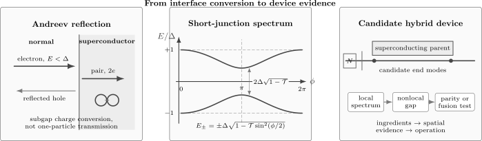
One interface process supports several distinct inferences. At an NS boundary, an incident electron can return as a hole while a Cooper pair enters the condensate. Two such boundaries confine phase-dependent Andreev levels; a channel with transmission has an avoided crossing at . A candidate Majorana device adds spin–orbit coupling, field, gates, and induced pairing, but the evidence must progress from local spectroscopy to a nonlocal gap and parity-sensitive operations.
Normal–Superconductor Interfaces
Section titled “Normal–Superconductor Interfaces”Electron–hole conversion
Section titled “Electron–hole conversion”Consider an excitation with incident from a clean normal metal. The superconducting bulk has no propagating quasiparticle state at that energy. At an ideal interface, the incident electron is converted into an outgoing hole. The missing electron represented by the hole, together with the incident electron, transfers a Cooper pair into the condensate.
Near a smooth Fermi surface,
Linearization about gives
and therefore
The hole group velocity is opposite to the velocity of the missing electron. Under the Andreev approximation
the reflected hole nearly retraces the incident electron path. This is retroreflection. Fermi-surface mismatch, anisotropy, strong spin polarization, an interface barrier, or a chemical potential near a band edge can invalidate the simple geometry.
In weakly doped graphene, the reflected hole may lie in the opposite band and emerge in a specular rather than retro direction. That is a Dirac-band kinematic effect, not a failure of charge- conversion. Graphene and Dirac Materials owns the valley and pseudospin structure needed to interpret it.
Andreev phase
Section titled “Andreev phase”For an ideal interface and the stated Nambu convention, a convenient subgap electron-to-hole amplitude is
Its magnitude is one. The first factor is the energy-dependent Andreev phase; the second records the condensate phase. Another Nambu basis can move signs or phases between amplitudes, but closed electron–hole trajectories depend only on gauge-invariant combinations.
For a perfectly transmitting, lossless single interface,
Above the gap, propagating Bogoliubov quasiparticles become available in the superconductor, so reflection no longer exhausts the scattering probabilities.
Andreev Reflection
Section titled “Andreev Reflection”Barrier and transparency
Section titled “Barrier and transparency”The Blonder–Tinkham–Klapwijk (BTK) model represents a short interface barrier by a dimensionless strength . In its matched, one-dimensional normal-state limit,
For a subgap excitation, zero temperature, and no lifetime broadening, the Andreev probability is
At zero energy this becomes
Subgap unitarity gives for the ordinary-reflection probability in this elementary model. The result shows why Andreev reflection is especially sensitive to a tunnel barrier: a low-transparency interface must transmit the two-particle conversion coherently.
Conductance and doubling
Section titled “Conductance and doubling”Let label spin-degenerate orbital channels. The zero-temperature NS conductance can be written
For subgap elastic reflection,
so
At zero energy, a normal scattering region with transmission eigenvalues gives
The corresponding normal conductance is
A perfectly open channel therefore changes from to . This conductance doubling is not universal for an imperfect contact. Series resistance, finite temperature, mode mixing, inelastic loss, and a soft gap can reduce or reshape it. Conductance Quantization owns the normal transmission-eigenvalue derivation and contact ledger.
At finite temperature, an ideal zero-temperature spectrum is thermally convolved:
Instrumental broadening, electromagnetic noise, and genuine quasiparticle lifetime effects are separate convolutions or self-energies. Replacing all of them by one phenomenological broadening parameter can fit a line shape without identifying its cause.
Transparent contact or tunnel spectrometer?
Section titled “Transparent contact or tunnel spectrometer?”In the high-barrier limit, current is dominated by single-quasiparticle tunneling and differential conductance can approximately follow the superconducting density of states. At high transparency, Andreev processes and multiple scattering dominate; the same density-of-states reading is invalid.
Useful diagnostics include:
- normal-state conductance and independently estimated channel transparencies;
- temperature and magnetic-field evolution of gap edges;
- excess current above the gap;
- shot noise or multiple-Andreev-reflection structure where applicable;
- consistency across barrier-gate settings;
- a calibrated series-resistance correction.
In an NSN geometry, an electron from one normal lead can emerge as a hole in the other lead, splitting a Cooper pair between contacts. Crossed Andreev reflection competes with elastic cotunneling, ordinary quasiparticle transport, and interaction effects. A nonlocal conductance sign by itself does not uniquely select one mechanism; the full bias, gate, field, and contact matrix is needed.
Andreev Bound States
Section titled “Andreev Bound States”Closed electron–hole trajectories
Section titled “Closed electron–hole trajectories”Two Andreev-reflecting boundaries can confine a subgap state. In a clean one-dimensional SNS segment of length , a schematic quantization rule is
where is the gauge-invariant phase difference and is an integer. The terms are, respectively, the two Andreev phases, the dynamical electron–hole phase in the normal region, and the condensate-phase difference.
The short-junction condition is most reliably stated using the dwell time:
or equivalently a Thouless scale
Geometric length alone is insufficient when a barrier or diffusive region makes the dwell time long.
Transmission-resolved spectrum
Section titled “Transmission-resolved spectrum”For a short, noninteracting junction with equal gap magnitudes and a normal-state transmission eigenvalue , the positive Andreev energy is
Particle–hole redundancy supplies branches at . In the absence of Zeeman or spin-active terms, each orbital level is also spin degenerate.
At ,
Thus imperfect transmission opens an avoided-crossing scale between the positive and negative branches. A perfectly transmitting ordinary channel reaches zero at in this ideal model. That crossing alone is not proof of topological superconductivity: its protection, degeneracy, parity dynamics, and response to allowed perturbations must be established.
Bound-state supercurrent
Section titled “Bound-state supercurrent”The phase derivative of the thermodynamic free energy produces current:
For an equilibrium spin-degenerate short-junction channel,
Low-transparency channels give an approximately sinusoidal current–phase relation. Highly transmitting channels are skewed because their levels disperse strongly near . The Josephson Effect develops the full phase, voltage, magnetic-interference, and circuit consequences.
Microwave spectroscopy can drive an even-parity pair transition with an ideal energy near . Odd-parity states correspond to one trapped quasiparticle and can block or shift allowed transitions. Spin–orbit coupling, Zeeman splitting, interactions, and coupling to a resonator enrich this simple four-state ledger.
The short-junction formula should not be stretched beyond its assumptions. Long ballistic and diffusive junctions contain many phase-dependent levels set by . Interacting quantum dots can undergo singlet–doublet or – transitions. A magnetic impurity produces Yu–Shiba–Rusinov physics. Those spectra require their own Hamiltonians rather than an effective transparency fitted after the fact.
Semiconductor–Superconductor Heterostructures
Section titled “Semiconductor–Superconductor Heterostructures”Induced pairing and renormalization
Section titled “Induced pairing and renormalization”A semiconductor does not inherit the parent order parameter unchanged. Integrating out an ideal wide-band -wave parent gives a model self-energy of the form
where measures interface coupling and is the parent gap. For ,
The same quasiparticle weight renormalizes semiconductor energy scales in this elementary model:
Stronger coupling can harden and enlarge the induced gap, but it can also reduce the effective semiconductor factor and spin–orbit energy, transmit disorder from the parent, and increase sensitivity to orbital depairing. The best interface is therefore not defined by alone.
Spatial pair-amplitude profiles, inverse proximity, coherence lengths, and quasiclassical Eilenberger or Usadel equations belong to Superconducting Proximity Effect. Here is a device parameter that must be inferred together with its spectral hardness, field dependence, and spatial uniformity.
Hard gap and device quality
Section titled “Hard gap and device quality”A hard gap means that subgap spectral weight is strongly suppressed relative to the above-gap response under a declared probe and resolution. It does not mean exactly zero density of states, and it does not by itself identify the cause of any remaining subgap conductance.
| Parameter | Why it matters | What must be measured or modeled |
|---|---|---|
| interface transparency | controls induced pairing and Andreev conversion | normal conductance, excess current, mode dependence |
| induced gap and hardness | protects low-energy states | temperature, field, barrier, and spatial dependence |
| carrier density and mode count | sets chemical potential and unwanted subbands | gate maps, electrostatic simulation, quantum oscillations |
| spin–orbit coupling | enables helical-state engineering | anisotropic spectroscopy and level anticrossings |
| effective Zeeman coupling | tunes spin structure and candidate transitions | tensor, field orientation, parent renormalization |
| disorder and smooth confinement | create ordinary subgap states | length dependence, multi-terminal and spatial probes |
| parent critical field | limits usable Zeeman and phase space | thin-film geometry, orbital response, hysteresis |
| quasiparticle parity lifetime | limits coherent operation | time-domain switching and poisoning statistics |
Tunneling conductance is proportional to a local density of states only in a controlled tunnel limit. An open probe measures a scattering problem. A gate-dependent soft gap can come from interface disorder, unintended dots, pair breaking, heating, or contact geometry; naming one mechanism requires discriminating controls.
Majorana Device Platforms
Section titled “Majorana Device Platforms”Hardware routes
Section titled “Hardware routes”The most direct device route combines a gate-tunable semiconductor, spin–orbit coupling, Zeeman splitting, and induced -wave pairing. A uniform single-band nanowire model has the reference criterion
on the topological side of a bulk gap closing, provided a reopened gap survives. This is a model locator, not a certification rule. Topological Superconductors derives the Hamiltonian and invariant and explains why multiband occupation, disorder, orbital field effects, finite length, smooth dots, and parent-gap collapse can invalidate the simple inequality.
| Platform | Additional control | Central device challenge |
|---|---|---|
| partially covered nanowire | local gates and field orientation | uniform chemical potential, hard gap, separated end modes |
| planar Josephson junction | superconducting phase difference | phase calibration, transverse modes, edge disorder |
| full-shell nanowire | flux-induced phase winding | Little–Parks sectors, core electrostatics, shell disorder |
| topological-insulator hybrid | spin-momentum-locked surface or edge | bulk conduction and interface transparency |
| quantum-dot or Andreev-state chain | programmable normal and crossed pairing links | scaling beyond a few tuned sites into a gapped phase |
These are candidate platforms. Demonstrating their ingredients is scientifically valuable even when the topological interpretation remains unsettled.
Evidence before labels
Section titled “Evidence before labels”An isolated Majorana mode coupled to one ideal normal channel can produce resonant zero-energy Andreev reflection with
at zero temperature. Ordinary Andreev bound states can also approach zero, remain pinned over a parameter range, and generate a similar local conductance. Disorder and smooth confinement broaden the set of alternatives.
A defensible device claim therefore asks:
- Does a bulk or nonlocal probe show a gap closing and reopening?
- Do both ends respond consistently while remaining spatially separated?
- Does the candidate zero mode remain below a measured excitation gap?
- Are temperature, broadening, lead channels, and series resistance calibrated?
- Are quantum-dot, disorder, level-crossing, and nonequilibrium explanations tested?
- Is fermion parity initialized, read out, and stable on the operation timescale?
- Has a fusion or braid-order protocol been distinguished from ordinary coherent dynamics?
Local spectroscopy is one part of that chain. The canonical Topological Superconductors article maintains the full evidence hierarchy and current status because those frontier claims evolve faster than the settled interface physics developed here.
Common Mistakes
Section titled “Common Mistakes”- Calling every subgap conductance feature Andreev reflection. Heating, leakage, quasiparticles, and ordinary resonances require controls.
- Assuming conductance always doubles below the gap. Exact doubling requires a perfectly open, coherent channel under the stated degeneracy convention.
- Reading density of states from a transparent contact. An open NS contact measures scattering, not simple tunnel spectroscopy.
- Treating a hole as a positive-charge particle with the same trajectory rules as an electron. It is a missing electron, and group velocity must be tracked explicitly.
- Using geometric length as the short-junction criterion. Dwell time and are the relevant scales.
- Fitting every Andreev level with one transparency. Spin, interactions, orbital structure, and energy-dependent scattering can invalidate the formula.
- Calling a zero at topological. A perfectly transmitting ordinary channel has such a crossing in the ideal short-junction model.
- Equating a hard induced gap with a topological gap. The latter requires a bulk invariant and a surviving reopened excitation gap.
- Using the nanowire inequality as a phase measurement. Its parameters are model-dependent and can change with field and coupling.
- Treating a local zero-bias peak as a Majorana proof. Ordinary Andreev states and disorder can mimic both persistence and near- height.
Exercises
Section titled “Exercises”1. Electron–hole momentum mismatch
Section titled “1. Electron–hole momentum mismatch”For and , estimate and the inverse mismatch length .
Solution
Using
with
gives
Therefore
The full relative-phase wavelength is . Stating which of these two lengths is meant avoids a common factor- ambiguity.
2. Barrier suppression
Section titled “2. Barrier suppression”A single interface has normal-state transparency . Find its zero-energy Andreev probability and the ratio of its subgap conductance to its normal conductance.
Solution
The Andreev probability is
For one spin-degenerate orbital mode,
Hence
The conductance is enhanced but not doubled.
3. Multichannel NS conductance
Section titled “3. Multichannel NS conductance”A short normal contact has two spin-degenerate transmission eigenvalues and . Find , , and their ratio.
Solution
The normal conductance is
For the NS contact,
Thus
One open mode doubles, while the partially transmitting mode does not.
4. Avoided crossing at phase pi
Section titled “4. Avoided crossing at phase pi”For a short-junction channel with , find the positive Andreev energy at and the separation between the positive and negative branches.
Solution
At ,
The two BdG branches lie at , so their separation is
The transmission is high, but the crossing is still avoided.
5. Derive the channel supercurrent
Section titled “5. Derive the channel supercurrent”At zero temperature, derive the equilibrium current carried by one spin-degenerate short-junction channel from its positive Andreev energy.
Solution
The occupied negative-energy branch contributes the phase-dependent ground-state energy
Therefore
Differentiating
gives
Thermal occupation multiplies this result by .
6. Coupling and induced gap
Section titled “6. Coupling and induced gap”In the elementary self-energy model, let . Find and . What happens to a bare semiconductor energy scale ?
Solution
The quasiparticle weight is
The induced gap is
Within this low-energy model,
The interface induces pairing and renormalizes the semiconductor at the same time.
7. Two-pi and four-pi statements
Section titled “7. Two-pi and four-pi statements”Why can a parity-resolved Andreev branch appear periodic while the equilibrium free energy remains periodic?
Solution
A protected crossing can exchange the ordering of two fixed-parity branches after . Following one parity branch without relaxation may therefore require to return to the same state. In equilibrium, the system occupies the lower available energy and may switch parity or branch at the crossing. The thermodynamic spectrum then repeats after .
A reported response must consequently state the drive frequency, parity lifetime, Landau–Zener probability, and nonequilibrium occupation. Missing Shapiro steps alone do not fix the mechanism.
8. Audit a zero-bias claim
Section titled “8. Audit a zero-bias claim”A proximitized nanowire shows a stable zero-bias peak near at one end over a finite field interval. Name four additional checks needed before interpreting it as a topological Majorana mode.
Solution
Useful checks include:
- a bulk or nonlocal measurement of gap closing and reopening;
- correlated but spatially separated behavior at both ends;
- stability below a measured excitation gap;
- calibrated temperature, broadening, lead-channel count, and series resistance;
- controls against smooth quantum dots, disorder, level crossings, and dissipation;
- length or spatial dependence consistent with separated end modes;
- parity lifetime and poisoning measurements;
- fusion or braid-order protocols with ordinary coherent alternatives excluded.
The local peak is compatible with resonant Andreev reflection from a Majorana mode, but the same observable is not unique to that mechanism.
Connections
Section titled “Connections”- BCS Theory supplies the parent gap, coherence factors, condensation scale, and weak-coupling limits.
- Bogoliubov Quasiparticles owns Nambu branch counting, particle–hole mixing, and quasiparticle normalization.
- Conductance Quantization develops normal transmission eigenvalues, degeneracy, contacts, and shot noise.
- Quantum Point Contacts provides gate-defined mode and barrier control for hybrid spectroscopy.
- Quantum Dots owns confinement, interactions, shell filling, and the ordinary discrete levels that can hybridize with a superconductor.
- Moiré Superconductivity separates intrinsic pairing evidence from proximity-induced gaps and uses Andreev and tunneling probes to interrogate tunable moiré condensates.
- Josephson Effect owns gauge-invariant phase dynamics, current–phase relations, Shapiro locking, SQUIDs, and environmental circuit behavior.
- Topological Superconductors owns BdG invariants, Majorana modes, engineered-platform classification, evidence hierarchy, and current frontier status.
- Graphene and Dirac Materials supplies the valley and pseudospin kinematics behind specular Andreev reflection.
- van der Waals Heterostructures owns generic stack assembly, alignment, gate architecture, and the distinction between hybridization-mediated proximity and electrostatic or dielectric interface effects.
- Engineered Heterostructures compares superconducting hybrids with magnetic–topological, oxide, and cavity interfaces and supplies the cross-platform phase-claim ladder.
- Single-Electron Devices explains pumps and hybrid-turnstile error channels, including Andreev transfer and quasiparticle poisoning.
- Nanostructures for Quantum Technology places hybrid spectra and parity primitives inside a measured control, error, fabrication, and architecture ledger.
- Mesoscopic Transport owns reservoir rates, counting statistics, detector records, and noise beyond coherent scattering.
References
Section titled “References”- A. F. Andreev, “The Thermal Conductivity of the Intermediate State in Superconductors,” Soviet Physics JETP 19, 1228–1231 (1964).
- G. E. Blonder, M. Tinkham, and T. M. Klapwijk, “Transition from Metallic to Tunneling Regimes in Superconducting Microconstrictions: Excess Current, Charge Imbalance, and Supercurrent Conversion,” Physical Review B 25, 4515–4532 (1982), doi:10.1103/PhysRevB.25.4515.
- C. W. J. Beenakker, “Quantum Transport in Semiconductor–Superconductor Microjunctions,” Physical Review B 46, 12841–12844 (1992), doi:10.1103/PhysRevB.46.12841.
- C. W. J. Beenakker, “Universal Limit of Critical-Current Fluctuations in Mesoscopic Josephson Junctions,” Physical Review Letters 67, 3836–3839 (1991), doi:10.1103/PhysRevLett.67.3836.
- C. W. J. Beenakker, “Specular Andreev Reflection in Graphene,” Physical Review Letters 97, 067007 (2006), doi:10.1103/PhysRevLett.97.067007.
- M. Hays, G. de Lange, K. Serniak, D. J. van Woerkom, D. Bouman, P. Krogstrup, J. Nygård, A. Geresdi, and M. H. Devoret, “Direct Microwave Measurement of Andreev-Bound-State Dynamics in a Semiconductor-Nanowire Josephson Junction,” Physical Review Letters 121, 047001 (2018), doi:10.1103/PhysRevLett.121.047001.
- L. Tosi, C. Metzger, M. F. Goffman, C. Urbina, H. Pothier, S. Park, A. Levy Yeyati, J. Nygård, and P. Krogstrup, “Spin-Orbit Splitting of Andreev States Revealed by Microwave Spectroscopy,” Physical Review X 9, 011010 (2019), doi:10.1103/PhysRevX.9.011010.
- W. Chang, S. M. Albrecht, T. S. Jespersen, F. Kuemmeth, P. Krogstrup, J. Nygård, and C. M. Marcus, “Hard Gap in Epitaxial Semiconductor–Superconductor Nanowires,” Nature Nanotechnology 10, 232–236 (2015), doi:10.1038/nnano.2014.306.
- P. Krogstrup et al., “Epitaxy of Semiconductor–Superconductor Nanowires,” Nature Materials 14, 400–406 (2015), doi:10.1038/nmat4176.
- M. Kjaergaard et al., “Quantized Conductance Doubling and Hard Gap in a Two-Dimensional Semiconductor–Superconductor Heterostructure,” Nature Communications 7, 12841 (2016), doi:10.1038/ncomms12841.
- R. M. Lutchyn, J. D. Sau, and S. Das Sarma, “Majorana Fermions and a Topological Phase Transition in Semiconductor–Superconductor Heterostructures,” Physical Review Letters 105, 077001 (2010), doi:10.1103/PhysRevLett.105.077001.
- Y. Oreg, G. Refael, and F. von Oppen, “Helical Liquids and Majorana Bound States in Quantum Wires,” Physical Review Letters 105, 177002 (2010), doi:10.1103/PhysRevLett.105.177002.
- V. Mourik et al., “Signatures of Majorana Fermions in Hybrid Superconductor–Semiconductor Nanowire Devices,” Science 336, 1003–1007 (2012), doi:10.1126/science.1222360.
- C.-X. Liu, J. D. Sau, T. D. Stanescu, and S. Das Sarma, “Andreev Bound States versus Majorana Bound States in Quantum Dot–Nanowire–Superconductor Hybrid Structures,” Physical Review B 96, 075161 (2017), doi:10.1103/PhysRevB.96.075161.
- A. Fornieri et al., “Evidence of Topological Superconductivity in Planar Josephson Junctions,” Nature 569, 89–92 (2019), doi:10.1038/s41586-019-1068-8.
- H. Ren et al., “Topological Superconductivity in a Phase-Controlled Josephson Junction,” Nature 569, 93–98 (2019), doi:10.1038/s41586-019-1148-9.
- H. Pan and S. Das Sarma, “Physical Mechanisms for Zero-Bias Conductance Peaks in Majorana Nanowires,” Physical Review Research 2, 013377 (2020), doi:10.1103/PhysRevResearch.2.013377.
Further reading
Section titled “Further reading”- C. W. J. Beenakker, “Random-Matrix Theory of Quantum Transport,” Reviews of Modern Physics 69, 731–808 (1997), doi:10.1103/RevModPhys.69.731.
- E. Prada et al., “From Andreev to Majorana Bound States in Hybrid Superconductor–Semiconductor Nanowires,” Nature Reviews Physics 2, 575–594 (2020), doi:10.1038/s42254-020-0228-y.