Coulomb Blockade
Coulomb blockade is the suppression of low-order charge transfer through a small, weakly contacted conductor because changing its integer charge costs electrostatic free energy. It is not merely a small conductance, a spectral gap, or a classical contact resistance. The diagnostic content lies in the dependence on gate charge, bias, temperature, and junction coupling.
The effect is simplest when an island is joined to source and drain by opaque tunnel barriers and coupled capacitively to a gate. The island can then remain in a definite charge sector long enough for the energy cost of one extra electron to control transport. Gate voltage shifts the relative energies of those sectors; source–drain voltage opens a transport window; tunnel events connect neighboring sectors.
This page is the canonical home for the orthodox capacitance-network ledger, free-energy changes of individual junction events, Coulomb-diamond slopes, and the operating principle of a single-electron transistor. Quantum Dots owns confinement spectra, orbital filling, and the constant-interaction addition spectrum. Mesoscopic Transport owns master equations, current noise, and counting statistics. Single-Electron Devices owns device engineering, charge sensing, pumps, turnstiles, and metrological error budgets.
Regime and Convention Ledger
Section titled “Regime and Convention Ledger”Two conventions must be declared before comparing formulas.
First, this page defines
so that the electrostatic energy is . The electrostatic contribution to the spacing between successive addition thresholds is
Some literature calls the charging energy. Neither convention is wrong, but silently switching between them creates a factor-of-two error.
Second, denotes the electrical potential of electrode , whereas an electron reservoir has electrochemical potential
Raising an electrode’s electrical potential therefore lowers its electron electrochemical potential. Coulomb-diamond slopes change sign if a different voltage or current convention is used.
The strict orthodox limit assumes:
and, for a normal tunnel junction,
Here is a tunneling rate, so is an energy width. These inequalities identify a controlled regime rather than sharp phase boundaries. Charge quantization is progressively renormalized and broadened as a contact opens.
| Scale or parameter | Role | Failure when it is too large or too small |
|---|---|---|
| separates neighboring charge thresholds | thermal and lifetime broadening wash out blockade when unresolved | |
| thermally populates uphill events | blockade valleys acquire activated current | |
| lifetime broadening from contact | neighboring charge sectors hybridize when broadening is strong | |
| dimensionless tunnel-coupling scale | higher-order tunneling and charge fluctuations grow as it approaches unity | |
| opens the transport window | sequential channels appear at diamond boundaries | |
| background charge | offsets the gate-induced charge | drift moves the entire pattern without changing the ideal period |
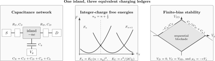
Three equivalent descriptions in the simplified three-capacitor model. Source, drain, and gate induce the offset charge of an island with integer excess-electron number . Neighboring electrostatic parabolas are degenerate at half-integer . With the drain grounded and source biased at , sequential-tunneling thresholds form diamond edges whose slopes are and . Additional stray capacitance changes the second denominator to .
Charging Energy
Section titled “Charging Energy”Capacitance network
Section titled “Capacitance network”Consider an island coupled capacitively to source, drain, gate, and any other conductors. Define
where collects stray and deliberately added capacitances not shown separately. After the linear capacitor degrees of freedom and the work done by ideal voltage sources are accounted for, the charge-dependent free energy can be written, up to an -independent term, as
with
is the integer number of excess electrons and is a static offset charge. A shift simply relabels the charge sectors. Slowly varying fluctuators instead produce charge-offset drift and low-frequency noise.
The free-energy cost to add the th excess electron is
Neighboring sectors are degenerate when
At zero source–drain bias, changing the gate voltage by
advances by one and returns the electrostatic problem to the same point in the next charge sector. This is the ideal gate period of Coulomb oscillations.
At the center of the th stability interval, , the costs to add or remove an electron are both
The second difference of the island energy is instead
That second difference is the electrostatic contribution to the addition-energy spacing measured between neighboring degeneracy points.
What the capacitance model omits
Section titled “What the capacitance model omits”A metallic island can have a level spacing much smaller than and still show charging effects. A few-electron semiconductor dot usually requires a discrete-spectrum term as well:
Then
contains orbital, exchange, valley, spin, and residual-interaction contributions. The capacitance model predicts the common electrostatic backbone; it does not prove equal peak spacing or identify an excited state. The full addition-spectrum interpretation is developed in Quantum Dots.
Charging-scale example
Section titled “Charging-scale example”Suppose the coefficient in the declared convention is
Then
The corresponding electrostatic addition increment is . A paper using would quote that latter number as its charging energy for the same device.
Tunnel Barriers
Section titled “Tunnel Barriers”Charging energy alone does not produce an observable transport blockade. The island must exchange charge slowly enough with its reservoirs that integer charge sectors remain meaningful, yet rapidly enough for a current to be measured.
Opaque-junction criterion
Section titled “Opaque-junction criterion”For a many-channel normal tunnel junction,
where every transmission eigenvalue satisfies . The dimensionless conductance is
The orthodox expansion is controlled when , equivalently . This resistance criterion concerns quantum charge fluctuations. It is distinct from the dynamical time constant and from the requirement that the measured current exceed an instrument’s noise floor.
An experimentally useful barrier therefore obeys competing demands:
for thermally broadened sequential tunneling, while
is needed to observe enough events in a measurement interval . Closing a barrier improves charge isolation but eventually makes transport impractically slow.
Free-energy ledger for one event
Section titled “Free-energy ledger for one event”For any proposed tunneling event, define
including the island and voltage-source work appropriate to that event. In the normal-metal orthodox approximation, a junction of resistance has rate
The zero-temperature limits expose the physics:
Downhill events occur; uphill events freeze out. At finite temperature,
which is local detailed balance.
As a scale estimate, take and a favorable event with at sufficiently low temperature. Then
and the associated energy width is only
A gigahertz event rate can therefore coexist with sub-microelectronvolt lifetime broadening. Rate and energy width must not be denoted by one unqualified symbol.
Sequential tunneling is not the whole current
Section titled “Sequential tunneling is not the whole current”Inside an ideal diamond, every first-order route contains an uphill step, so sequential current is thermally suppressed. The measured current need not vanish:
- elastic cotunneling transfers charge through a virtual island state without exciting the island;
- inelastic cotunneling leaves an excitation behind once sufficient bias is available;
- Kondo correlations can restore a zero-bias resonance in an odd-occupation valley;
- photon- or phonon-assisted tunneling exchanges energy with another mode;
- leakage paths or unintended islands can mimic a residual blockade current.
These mechanisms have distinct temperature, bias, magnetic-field, and barrier-coupling dependences. A dark region in a conductance map establishes suppressed conductance, not by itself the microscopic reason.
An electromagnetic environment can also absorb or supply energy during tunneling. This dynamical Coulomb blockade is described by an environmental energy-exchange distribution such as . It is related historically and mathematically to charging physics, but it is not identical to the static integer-charge blockade of a double-junction island.
Coulomb Diamonds
Section titled “Coulomb Diamonds”A Coulomb diamond is a low-conductance region in a map of differential conductance,
versus gate voltage and source–drain bias. Its boundaries are alignments between an island charge-transition electrochemical potential and a reservoir electrochemical potential.
Deriving the edge slopes
Section titled “Deriving the edge slopes”Choose the explicit convention
so
For one transition, absorb the charge index, offset charge, and voltage-independent microscopic energies into . The island transition is
The drain-alignment edge satisfies
Differentiating along that line gives
The source-alignment edge satisfies
and therefore
For the three-capacitor model with ,
The slope labels swap if the opposite lead is biased, and both signs can flip if the plotted bias is defined oppositely. Published slope formulas are meaningful only with their bias convention attached.
The gate lever arm is
so a small horizontal gate displacement at fixed lead voltages changes the transition energy by
This conversion is often more reliable than treating the full vertical diamond height as simply an energy divided by . Bias voltage is partitioned capacitively, and the partition depends on which electrode is driven.
Extracting capacitances from a diamond
Section titled “Extracting capacitances from a diamond”Suppose a stability diagram made with the convention above has:
The gate period gives
The negative edge gives
and the positive edge gives
If stray capacitance is negligible, then
so
The declared charging coefficient is then
If is appreciable, the two slopes determine and the combination , not alone. A three-capacitor fit would then be overinterpreted.
Reading structure beyond the edges
Section titled “Reading structure beyond the edges”| Feature in a stability diagram | Leading interpretation | Corroborating checks |
|---|---|---|
| repeated closed diamonds | stable integer charge sectors | one-electron gate periodicity, reproducible edge slopes, thermal activation |
| lines parallel to an edge outside blockade | additional island transition or excitation | magnetic-field evolution, temperature dependence, repetition across charge sectors |
| threshold inside a blockade region | inelastic cotunneling onset | weak gate dependence within one valley, barrier-order scaling |
| zero-bias ridge in an odd valley | possible Kondo resonance | odd–even pattern, logarithmic temperature evolution, Zeeman splitting |
| shifted duplicate diamonds | second island or charge rearrangement | abrupt offset jumps, multiple slope families, hysteresis |
| rounded or absent vertices | thermal broadening, lifetime broadening, noise, or open contacts | compare temperature and barrier-gate sweeps |
Diamond edges establish energetic alignment. They do not by themselves identify spin, valley, phonon, or orbital character. That assignment needs a controlled perturbation and a model whose parameters remain consistent across the map.
Single-Electron Transistor
Section titled “Single-Electron Transistor”A normal-state single-electron transistor consists of one island, two tunnel junctions, and at least one gate capacitor. The gate modulates a source–drain current without ideally drawing a dc gate current.
At zero bias, adjacent charge states are degenerate whenever
Near such a point, both directions of a sequential cycle can become energetically accessible, producing a conductance peak. Near integer , the island lies in the middle of a stable charge sector and sequential conductance is suppressed. Repeating this pattern gives Coulomb oscillations with ideal period
The useful transfer quantity is the transconductance
It is largest on the side of a conductance peak rather than at the current maximum. A nearby charge changes the effective offset charge and moves the operating point, which is why a single-electron transistor can act as an electrometer.
The word transistor should not conceal the differences from a field-effect transistor:
| Conventional field-effect transistor | Single-electron transistor |
|---|---|
| gate controls a continuous carrier-density barrier | gate shifts discrete charge degeneracies |
| transfer curve usually has one main turn-on | ideal transfer curve is periodic |
| operation need not resolve -scale charge | operation relies on charge quantization |
| room-temperature operation is common | temperature must remain below the relevant charging scale |
| offset charge mainly shifts a threshold | one-electron offset shifts an entire oscillation period |
The ideal periodic picture is modified by background-charge motion, cotunneling, barrier asymmetry, finite level spacing, superconductivity, nonequilibrium heating, and the impedance of the external circuit. Charge sensitivity, radio-frequency embedding, pumps, turnstiles, and metrological accuracy require a device-level noise and error ledger; they are not implied by the existence of a Coulomb peak.
Quantum Dots and Qubits
Section titled “Quantum Dots and Qubits”Coulomb blockade is a transport regime, not a material class. Its microscopic content depends on the island.
| Island platform | What is quantized | Important additions to the orthodox model |
|---|---|---|
| normal-metal grain | total excess charge | dense quasiparticle spectrum, environmental impedance |
| gate-defined semiconductor dot | charge plus resolvable orbitals | spin, valley, exchange, spin–orbit coupling |
| nanowire, nanotube, or molecular dot | charge and confined longitudinal states | shells, vibrations, contact-dependent hybridization |
| superconducting island | charge parity and condensate phase | gap, quasiparticle poisoning, Josephson coupling, possible periodicity |
| unintended disorder island | localized charge | unstable capacitances and multiple overlapping diamonds |
For a spin qubit, blockade can stabilize a chosen electron number and provide the charge-sector map used for initialization and readout. It does not establish coherent control. Demonstrating a qubit additionally requires a two-level encoding, calibrated manipulation, state-selective measurement, and coherence or fidelity evidence.
Pauli spin blockade is also distinct. Coulomb blockade forbids a charge transition because no energetically allowed charge state lies in the transport window. Pauli blockade forbids or slows a transition because spin symmetry excludes the accessible final state even when the charge configuration is energetically allowed. Spin Qubits develops that distinction in the context of preparation, control, and readout.
Superconducting circuits provide another important boundary. A superconducting island can exhibit charging effects, but coherent Cooper-pair tunneling introduces a Josephson energy that competes with . The spectrum then depends on both charge and phase; ordinary normal-state sequential tunneling is no longer a complete description.
Nearby phenomena that are not interchangeable
Section titled “Nearby phenomena that are not interchangeable”| Name | What is suppressed | Primary mechanism |
|---|---|---|
| Coulomb blockade | low-order transfer onto an integer-charge island | electrostatic cost plus weak contacts |
| Pauli blockade | a spin-selective transition | fermionic symmetry and selection rules |
| Coulomb gap | low-energy single-particle density of states in a disordered interacting system | long-range interactions and localization |
| dynamical Coulomb blockade | low-energy tunneling through a junction in a circuit | energy exchange with electromagnetic modes |
| superconducting gap blockade | quasiparticle current below a gap threshold | pairing spectrum |
| photon blockade | occupation of a nonlinear optical mode | anharmonic level spacing |
Similar current suppression does not make these mechanisms equivalent. Gate periodicity, bias thresholds, symmetry dependence, environmental impedance, and spectroscopy distinguish them.
Common Mistakes
Section titled “Common Mistakes”- Calling every low-current region Coulomb blockade. Contact depletion, a band gap, localization, a superconducting gap, and instrument floor can all suppress current.
- Using “charging energy” without declaring the factor of two. State whether it means or .
- Equating diamond height with addition energy by inspection. First declare which lead is biased and include capacitive division.
- Confusing tunneling rate and energy broadening. A rate becomes an energy only after multiplication by .
- Treating as a thermal criterion. It controls quantum charge fluctuations; is the separate thermal condition.
- Assigning every parallel line to an excited orbital. Lead resonances, phonons, and unintended dots can produce similar slopes.
- Claiming perfect isolation from a dark diamond. Cotunneling and other higher-order processes remain possible.
- Equating charge stability with qubit coherence. A well-defined charge sector is useful infrastructure, not a coherence measurement.
Exercises
Section titled “Exercises”1. Degeneracy of neighboring charge sectors
Section titled “1. Degeneracy of neighboring charge sectors”Starting from
show that at . Find the cost to add an electron at the center of the th stability interval.
Solution
Set the two parabolas equal:
Subtracting the left side from the right gives
so
At ,
The central barrier to either neighboring sector is therefore in the convention used here.
2. Capacitance from a charging scale
Section titled “2. Capacitance from a charging scale”An experiment quotes using . Find and the electrostatic addition increment.
Solution
The capacitance is
The electrostatic second difference is
A source using as its definition would quote as the charging energy.
3. Gate period and offset charge
Section titled “3. Gate period and offset charge”A device has . Find the ideal Coulomb-oscillation period. If a fluctuator changes by , by what fraction of one period does the pattern shift?
Solution
The period is
Because , keeping fixed requires
Thus
The pattern shifts by of a period, in the direction opposite to the offset-charge change.
4. Diamond slopes
Section titled “4. Diamond slopes”The drain is grounded and the source is biased. A diamond has slopes and , and its gate period gives . Find and . If , find and .
Solution
Using the declared convention,
so
The positive edge gives
hence
If , then
and
Without the assumption, the data determine rather than separately.
5. Detailed balance of the orthodox rate
Section titled “5. Detailed balance of the orthodox rate”For
show that . Interpret the result for .
Solution
Write . Apart from the common prefactor,
whereas
Therefore
For , the forward event raises free energy and is Boltzmann-suppressed relative to its downhill reverse.
6. Rate, broadening, and thermal resolution
Section titled “6. Rate, broadening, and thermal resolution”A junction produces a tunneling rate at . Compare and in microelectronvolts. Is the resonance predominantly lifetime broadened in this comparison?
Solution
The lifetime width is
The thermal scale is
Thus
Within this comparison the line is thermally, not lifetime, broadened. A complete conclusion would also check voltage noise and the intrinsic excitation spacing.
7. Classifying a blockade
Section titled “7. Classifying a blockade”For each observation, name the leading mechanism and one discriminating test:
- A conductance dip through one tunnel junction deepens when the series environmental impedance is increased.
- A double dot carries current for one bias polarity but becomes trapped in a triplet configuration for the opposite polarity.
- A disordered insulator develops a soft suppression of tunneling density of states near the Fermi level.
- A gated island shows periodic peaks and closed diamonds.
Solution
- The leading interpretation is dynamical Coulomb blockade. Varying the impedance spectrum or measuring environmental sidebands tests energy exchange with the circuit.
- This is Pauli spin blockade. Magnetic-field dependence, spin relaxation, or spin-resonance lifting distinguishes the spin selection rule.
- This is a Coulomb gap. Its density-of-states scaling and dependence on disorder and dimensionality distinguish it from an island charging diagram.
- This is ordinary island Coulomb blockade. The one-electron gate period, capacitance-consistent slopes, and thermal activation provide quantitative checks.
The shared word blockade describes suppressed response, not a shared microscopic Hamiltonian.
8. What blockade proves for a qubit
Section titled “8. What blockade proves for a qubit”A semiconductor device displays a clean one-electron stability region and a charge-sensor signal for loading one electron. Which qubit claims are supported, and what remains to be demonstrated?
Solution
The data support controlled charge occupation, an estimate of addition energies, and a working charge-sensitive measurement channel. They may also identify a gate region suitable for isolating a spin.
They do not by themselves establish a qubit. One must still identify the encoded two-level subspace, demonstrate state preparation and calibrated control, measure state-selective readout, quantify relaxation and coherence, and report fidelity or error evidence appropriate to the claimed operation. Coulomb blockade supplies charge-sector infrastructure; it is not a coherence experiment.
Connections
Section titled “Connections”- Quantum Dots develops confinement, shell filling, orbital contributions to addition energies, and spectroscopy beyond the metallic-island model.
- Single-Electron Devices turns the blockade ledger into electrometers, event-resolved detectors, pumps, turnstiles, and uncertainty-aware current standards.
- Mesoscopic Transport derives sequential master equations, stationary current, shot noise, and full counting statistics.
- Quantum Point Contacts treats a nearby constriction as a charge detector, including responsivity, bandwidth, and backaction.
- Conductance Quantization gives the transmission-eigenvalue language needed as a tunnel contact becomes open.
- Quantum Coherence in Conductors separates phase coherence, escape, thermal averaging, and energy relaxation.
- Anderson Insulators distinguishes the distributed soft Coulomb gap and hopping network from discrete-island charging thresholds.
- Kondo Effect owns the correlated zero-bias resonance that can appear in an odd Coulomb valley.
- Anderson Impurity Model supplies the interacting-level model connecting Coulomb valleys, mixed valence, and local moments.
- Chemical Potential distinguishes reservoir electrochemical potentials from finite-system addition thresholds.
- Spin Qubits covers spin-to-charge conversion, Pauli blockade, coherent control, and readout evidence.
- Condensed Matter Roadmap places charging phenomena after quantum statistics and transport and before device-specific qubit engineering.
References
Section titled “References”- D. V. Averin and K. K. Likharev, “Coulomb Blockade of Single-Electron Tunneling, and Coherent Oscillations in Small Tunnel Junctions,” Journal of Low Temperature Physics 62, 345–373 (1986), doi:10.1007/BF00683469.
- T. A. Fulton and G. J. Dolan, “Observation of Single-Electron Charging Effects in Small Tunnel Junctions,” Physical Review Letters 59, 109–112 (1987), doi:10.1103/PhysRevLett.59.109.
- U. Meirav, M. A. Kastner, and S. J. Wind, “Single-Electron Charging and Periodic Conductance Resonances in GaAs Nanostructures,” Physical Review Letters 65, 771–774 (1990), doi:10.1103/PhysRevLett.65.771.
- C. W. J. Beenakker, “Theory of Coulomb-Blockade Oscillations in the Conductance of a Quantum Dot,” Physical Review B 44, 1646–1656 (1991), doi:10.1103/PhysRevB.44.1646.
- M. A. Kastner, “The Single-Electron Transistor,” Reviews of Modern Physics 64, 849–858 (1992), doi:10.1103/RevModPhys.64.849.
- H. Grabert and M. H. Devoret, eds., Single Charge Tunneling: Coulomb Blockade Phenomena in Nanostructures, NATO ASI Series B, vol. 294, Plenum Press, 1992, doi:10.1007/978-1-4757-2166-9.
- G.-L. Ingold and Yu. V. Nazarov, “Charge Tunneling Rates in Ultrasmall Junctions,” in Single Charge Tunneling, pp. 21–107, Plenum Press, 1992, doi:10.1007/978-1-4757-2166-9_2.
- H. van Houten, C. W. J. Beenakker, and A. A. M. Staring, “Coulomb-Blockade Oscillations in Semiconductor Nanostructures,” in Single Charge Tunneling, pp. 167–216, Plenum Press, 1992, doi:10.1007/978-1-4757-2166-9_5.
- D. V. Averin and Yu. V. Nazarov, “Macroscopic Quantum Tunneling of Charge and Co-Tunneling,” in Single Charge Tunneling, pp. 217–247, Plenum Press, 1992, doi:10.1007/978-1-4757-2166-9_6.
- K. K. Likharev, “Single-Electron Devices and Their Applications,” Proceedings of the IEEE 87, 606–632 (1999), doi:10.1109/5.752518.
- M. H. Devoret, D. Esteve, H. Grabert, G.-L. Ingold, H. Pothier, and C. Urbina, “Effect of the Electromagnetic Environment on the Coulomb Blockade in Ultrasmall Tunnel Junctions,” Physical Review Letters 64, 1824–1827 (1990), doi:10.1103/PhysRevLett.64.1824.
- Y. V. Nazarov, “Coulomb Blockade without Tunnel Junctions,” Physical Review Letters 82, 1245–1248 (1999), doi:10.1103/PhysRevLett.82.1245.
- W. G. van der Wiel, S. De Franceschi, J. M. Elzerman, T. Fujisawa, S. Tarucha, and L. P. Kouwenhoven, “Electron Transport through Double Quantum Dots,” Reviews of Modern Physics 75, 1–22 (2002), doi:10.1103/RevModPhys.75.1.
- R. Hanson, L. P. Kouwenhoven, J. R. Petta, S. Tarucha, and L. M. K. Vandersypen, “Spins in Few-Electron Quantum Dots,” Reviews of Modern Physics 79, 1217–1265 (2007), doi:10.1103/RevModPhys.79.1217.
Further reading
Section titled “Further reading”- C. W. J. Beenakker and H. van Houten, “Quantum Transport in Semiconductor Nanostructures,” Solid State Physics 44, 1–228 (1991), doi:10.1016/S0081-1947(08)60091-0.
- T. Ihn, Semiconductor Nanostructures: Quantum States and Electronic Transport, Oxford University Press, 2010, doi:10.1093/acprof:oso/9780199534425.001.0001.