Quantum Dots
A quantum dot is a finite region that confines mobile charge carriers in every spatial direction strongly enough that its low-energy orbital spectrum is discrete. The phrase zero-dimensional refers to that discrete spectrum, not to a geometrical point. A real dot has finite size, interfaces, gates, electromagnetic surroundings, and often tunnel contacts to reservoirs.
Quantum dots are called artificial atoms because they exhibit orbitals, shell filling, spin states, and an addition spectrum. The analogy is useful but incomplete. Their confinement is engineered rather than Coulombic, their charging energy depends on a device capacitance, their shape and carrier number can be tuned, and their coupling to leads or photons can be changed in situ.
This page owns the material and device ledger: confinement, orbital and charging contributions to addition energies, spin filling, and the distinction between transport and optical dots. It gives a first encounter with blockade spectroscopy; Coulomb Blockade owns the orthodox junction free-energy ledger, tunneling-rate criterion, and capacitance extraction from diamond slopes. Quantum Wires owns the limit with transverse subbands but extended longitudinal propagation; Quantum Point Contacts owns nearby charge-sensor responsivity, bandwidth, event counting, and detector backaction; Quantum Coherence in Conductors owns orbital phase memory and interference-based extraction; Mesoscopic Transport owns the reservoir master equations; Charged Harmonic Oscillator in a Magnetic Field owns the Fock–Darwin single-particle spectrum; Kondo Effect owns low-temperature impurity scaling; and Spin Qubits owns coherence, control, and readout protocols.
What Counts as a Quantum Dot?
Section titled “What Counts as a Quantum Dot?”Different platforms share discrete confinement but need not share the same dominant observable.
| Platform | Confinement mechanism | Common observable | Important extra physics |
|---|---|---|---|
| gate-defined semiconductor dot | electrostatic gates in a two-dimensional electron or hole system | dc or radio-frequency charge transport | capacitance network, reservoirs, valley and spin–orbit structure |
| etched or nanowire dot | material boundaries plus local gates or barriers | Coulomb diamonds and excited-state lines | surface disorder and longitudinal subbands |
| carbon nanotube or graphene dot | barriers, edges, band gap, or electrostatic confinement | transport and charge sensing | valley, sublattice, contact, and shell degeneracies |
| metallic island or molecule | tunnel junctions and finite capacitance | single-electron tunneling | dense orbital spectrum, vibrations, image charge |
| self-assembled epitaxial dot | strain and band offsets | absorption, resonance fluorescence, photoluminescence | excitons, fine structure, nuclear spins |
| colloidal nanocrystal | finite crystallite and dielectric interfaces | optical spectra and charge transfer | surface chemistry, dielectric mismatch, Auger processes |
An isolated defect center can also have discrete localized states, but “quantum dot” usually emphasizes an engineered or nanoscale confined region rather than one atomic defect. Conversely, a lithographic island is not automatically a useful quantum dot: if thermal broadening, disorder, or contact broadening washes out its discrete spectrum, a classical island or open conductor may be the better description.
Energy-Scale Ledger
Section titled “Energy-Scale Ledger”The correct model is selected by an ordering of scales, not by the device name. The central quantities are:
and
Here denotes an energy broadening unless a lowercase tunneling rate is explicitly introduced. This distinction prevents the common dimensional error of comparing a rate directly with an energy.
| Hierarchy | Resolved behavior |
|---|---|
| individual orbitals can be spectroscopically resolved | |
| charge states can be Coulomb blockaded | |
| linear-response addition peaks | |
| finite-bias charge and excited-state spectroscopy | |
| lifetime broadening and coherent resonant tunneling matter | |
| charge is no longer sharply quantized | |
| , exchange, or spin–orbit scale | spin or avoided-crossing structure can be resolved |
The addition energy is not generally equal to or . It is a many-electron energy difference that can contain both orbital and electrostatic contributions.
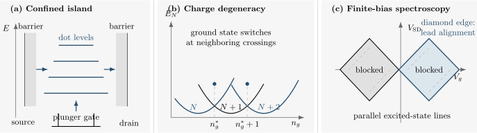
Three views of one transport dot. A confined island has discrete levels and tunnel barriers to source and drain; a plunger gate shifts its electrochemical potential. In the constant-interaction model, neighboring charge parabolas cross at charge-degeneracy points. At finite source–drain bias, blockade regions form Coulomb diamonds; their boundaries align a dot transition with a lead, while parallel lines outside the diamonds can reveal excited states.
Confined-Orbital Spectrum
Section titled “Confined-Orbital Spectrum”An effective-mass model for carriers in a semiconductor dot begins with
, , spin–orbit coupling, dielectric screening, and even the number of valley minima are material dependent. includes band offsets and electrostatic gates after the semiconductor boundary-value problem has been solved. A drawn gate voltage is therefore not itself the confinement potential.
Harmonic benchmark
Section titled “Harmonic benchmark”For an anisotropic two-dimensional harmonic approximation,
the spinless one-particle energies at are
A circular dot has and ideal shell degeneracies. Ellipticity, disorder, spin–orbit coupling, valley splitting, and interactions break or reorganize those degeneracies. In perpendicular field, the orbital benchmark becomes the Fock–Darwin spectrum.
For a large ballistic two-dimensional dot of electronic area , a rough mean spacing near the Fermi energy is
where counts unresolved internal degeneracy. This is an average density-of-states estimate, not a prediction of individual spacings. Shape, chaos, integrability, and interactions determine the fluctuations around it.
Coupling the Dot to Leads and Gates
Section titled “Coupling the Dot to Leads and Gates”A transport device adds source and drain reservoirs:
with
The lead-induced width of orbital is
The wide-band approximation treats this width as nearly constant over the energy window being measured. It can fail near a band edge, superconducting gap, resonant contact, or structured nanowire subband.
A plunger gate shifts dot electrochemical potentials. In a capacitance model,
and the gate lever arm is
For a small gate change that does not reshape the wavefunctions,
Barrier gates often change both the tunnel coupling and the dot potential. Treating every gate as a pure one-parameter control can therefore misidentify lever arms and linewidths.
Constant-Interaction Model
Section titled “Constant-Interaction Model”The constant-interaction model separates a fixed one-particle spectrum from a classical capacitance energy. Let
where spin is included in the orbital label . Define the dimensionless induced charge
Then
This convention calls the charging energy. Some literature instead calls the charging energy. Every numerical comparison must check that factor of two.
For the ground state with the lowest spin-orbitals occupied,
The electrochemical potential for adding the th electron is
The difference between successive addition thresholds is
Thus an addition spectrum contains both the next-orbital cost and the electrostatic cost. If two opposite spins fill the same orbital, the first term can be small; when a new shell starts, it can be large.
What the model neglects
Section titled “What the model neglects”The constant-interaction model assumes one capacitance independent of and a fixed orbital spectrum. It omits:
- exchange and correlation changes between charge sectors;
- gate-induced wavefunction deformation;
- occupation-dependent screening and quantum capacitance;
- image-charge and dielectric-interface corrections;
- level-dependent tunnel coupling;
- nonequilibrium population and relaxation;
- superconducting, ferromagnetic, or strongly structured leads.
It is a controlled ledger only when those corrections are smaller than the resolution required by the question.
Coulomb Blockade
Section titled “Coulomb Blockade”This section introduces the transport signature for the dot platform. The dedicated Coulomb Blockade article derives event free energies, orthodox rates, bias-convention-dependent edge slopes, and the single-electron-transistor operating principle.
Let the source and drain have electrochemical potentials and . A sequential tunneling event is energetically allowed when a dot addition threshold lies in the transport window. For ,
If no accessible lies in that interval, first-order tunneling is blocked. At small bias, sweeping brings successive charge degeneracies through the common lead chemical potential and produces conductance peaks separated by blockade valleys.
Charge quantization is sharp when
and, in the orthodox tunnel-junction regime, when the effective barrier resistance is large compared with
These are regime criteria, not hard phase boundaries. Coherent quantum fluctuations progressively smear charge sectors as coupling increases.
Simplest sequential peak
Section titled “Simplest sequential peak”For one nondegenerate transition with tunneling rates and , the stationary current in the simplest rate model is
In linear response at equal lead temperatures,
where
The thermal full width at half maximum is
In gate voltage,
Spin degeneracy, excited states, nonequilibrium occupation, lifetime broadening, and energy-dependent barriers change the peak height or shape. A fitted width should therefore be called a temperature only after the regime has been validated.
Coulomb Diamonds
Section titled “Coulomb Diamonds”Plotting differential conductance
against and produces a charge-stability diagram. Regions with fixed integer occupation and no sequential transport appear as low-conductance diamonds. A diamond boundary occurs when an addition or removal electrochemical potential aligns with a lead:
The slopes depend on the complete capacitance matrix and on which lead is biased. The vertical extent gives an addition-energy scale only after the voltage convention and capacitive division are included. The gate spacing gives
only in the constant-interaction limit with negligible changes in orbital spacing.
Lines parallel to diamond edges can indicate transport through excited states. They can also arise from lead density-of-states features, barrier resonances, phonon-assisted processes, or a second unintended dot. Excited-state assignment requires reproducible slopes, magnetic-field evolution, temperature and tunnel-coupling dependence, and consistency across charge sectors.
Transport Regimes Beyond Sequential Tunneling
Section titled “Transport Regimes Beyond Sequential Tunneling”One device can move through several theories as gates and temperature change.
| Regime | Scale hierarchy | Appropriate description |
|---|---|---|
| nearly isolated dot | equilibrium addition spectrum or capacitance spectroscopy | |
| sequential tunneling | population rate equation | |
| lifetime-broadened resonance | coherent resonant-level or Green-function treatment | |
| cotunneling | sequential channel blockaded but virtual states accessible | higher-order tunneling |
| Kondo valley | odd local moment and | interacting Anderson or Kondo model |
| open dot | comparable with level or charging scales | scattering, random-matrix, or open-cavity description |
For one noninteracting spin-degenerate level with energy widths and ,
At zero temperature, the coherent two-terminal conductance is
This is not the thermal sequential peak above. The two formulas use different assumptions and even different meanings of unless rates and energy widths are carefully converted.
Conductance Quantization owns the multichannel Landauer staircase, degeneracy, contact-resistance, and transmission-eigenvalue ledger for open constrictions.
Anderson and Kondo regimes
Section titled “Anderson and Kondo regimes”A single interacting orbital is described by
The first and second addition thresholds are
When
and charge fluctuations are weak, the dot carries an odd-occupancy local moment. At sufficiently low temperature, coherent spin exchange with the leads can produce Kondo-enhanced conductance inside a valley that sequential tunneling would call blockaded.
Anderson Impurity Model owns the correlated spectral function and regime map. Kondo Effect owns scaling with temperature, bias, and magnetic field. A zero-bias peak alone does not establish Kondo physics.
Shell Filling, Spin, and Magnetic Spectroscopy
Section titled “Shell Filling, Spin, and Magnetic Spectroscopy”Pauli exclusion allows at most one fermion in each complete spin-orbital. In a weakly interacting picture, two electrons of opposite spin can occupy one spatial orbital. The addition energy then often alternates between:
- adding the partner spin to an occupied spatial orbital;
- starting a new orbital and paying an extra spacing.
Real few-electron dots can depart from this simple even–odd pattern because exchange favors spin alignment, valley states enlarge shells, spin–orbit coupling mixes quantum numbers, and correlations rearrange the ground state. A circular harmonic dot ideally closes shells at characteristic electron numbers, but observing a large addition energy is not sufficient by itself to identify a shell closure.
Magnetospectroscopy follows or excited-state lines. Slopes and avoided crossings can reveal:
orbital magnetic moments, singlet–triplet crossings, spin–orbit gaps, or valley splittings. Extracting requires separating orbital motion and gate-dependent lever arms from the Zeeman contribution.
Quantum Dots as Spin-Qubit Devices
Section titled “Quantum Dots as Spin-Qubit Devices”Few-electron dots provide electrically tunable charge and spin states. Common encodings include:
- one electron spin in one dot;
- a singlet–triplet subspace in a double dot;
- exchange-only encodings across three spins;
- hole-spin and spin–valley variants.
Tunnel coupling between two dots hybridizes charge states. In the one-particle basis ,
with eigenenergy splitting
Charge admixture enables rapid electrical control but also converts charge noise into qubit-frequency noise. Pauli spin blockade and spin-selective tunneling convert spin information into charge information for readout. These are powerful mechanisms, not automatic evidence of a high-fidelity qubit: initialization error, leakage, valley or orbital states, hyperfine fields, charge noise, phonons, and sensor backaction remain.
Tight-Binding Dimer owns the two-state hybridization algebra. Spin Qubits owns , , control filters, leakage, and readout fidelity.
Optical Quantum Dots
Section titled “Optical Quantum Dots”Self-assembled and colloidal quantum dots are often probed optically rather than by source–drain transport. Optical excitation creates an electron–hole pair. A schematic neutral-exciton transition energy is
where is the host or effective gap, and are confinement energies, is the electron–hole attraction, and represents fine-structure corrections. Charged excitons, biexcitons, dielectric mismatch, strain, and configuration mixing require a many-particle treatment.
The emitted photon energy is a difference between initial and final many-body states:
It is therefore unsafe to read a photoluminescence line as one bare electron orbital. Polarization, power dependence, charge tuning, photon correlations, lifetime, and magnetic-field response are needed to assign exciton complexes and fine structure.
Optical dots can emit antibunched photons and can host optically controlled spins, but material inhomogeneity, blinking, spectral diffusion, phonon sidebands, nonradiative decay, and extraction efficiency matter. Spontaneous Emission owns the radiative rate framework, while Antibunching owns the photon-correlation diagnostic.
Measurement Ledger
Section titled “Measurement Ledger”| Measurement | Directly observed | Common inference | Main caution |
|---|---|---|---|
| linear conductance versus gate | addition peaks | charge degeneracy and thermal width | barrier transmission and degeneracy affect height |
| finite-bias stability diagram | differential-conductance lines | addition energies and excited states | capacitance conversion and lead resonances |
| nearby charge sensor | changes in dot occupation | charge transition even without dot current | sensor backaction and cross-capacitance |
| radio-frequency reflectometry | impedance-dependent phase or amplitude | fast charge susceptibility and tunneling | resonator calibration and bandwidth |
| magnetospectroscopy | field-dependent transition lines | spin, orbital, valley, or exchange energies | lever-arm drift and orbital contributions |
| photoluminescence or resonance fluorescence | photon energy and statistics | excitons, fine structure, optical selection | final-state and spectral-diffusion effects |
A transport line is a transition between many-body charge states, not a direct photograph of a wavefunction. A charge sensor measures occupation susceptibility, not necessarily current. An optical line measures a radiative energy difference. Naming the operator and transition is the shortest route to a trustworthy interpretation.
Interpretation Workflow
Section titled “Interpretation Workflow”- Identify the platform. State whether confinement is gate-defined, structural, molecular, metallic, self-assembled, or colloidal.
- List resolved scales. Compare , , , , , Zeeman energy, and known valley or spin–orbit scales.
- Declare coupling units. Say whether is an energy width or is a transition rate.
- Calibrate electrostatics. Extract a capacitance model and gate lever arm before converting volts to energy.
- Assign charge states. Use transport together with charge sensing where possible; a conductance valley alone does not determine absolute occupation.
- Separate ground and excited transitions. Check slopes, magnetic evolution, and reproducibility across neighboring diamonds.
- Choose the transport theory. Distinguish sequential tunneling, cotunneling, coherent resonance, Kondo transport, and an open cavity.
- Report the measurement transition. Specify initial and final many-body states for electrical or optical spectroscopy.
- Test alternatives. Rule out unintended dots, lead resonances, heating, photon-assisted tunneling, and sensor artifacts.
Common mistakes
Section titled “Common mistakes”- Calling a dot zero-dimensional without stating the energy window in which all spatial subbands are frozen out.
- Equating charging energy with the electrostatic addition cost .
- Calling every Coulomb-diamond line a dot excited state.
- Reading gate voltage directly as energy without a lever arm.
- Mixing a tunneling rate with an energy broadening.
- Using a sequential rate equation after lifetime broadening or coherence becomes important.
- Assuming a closed-system orbital eigenvalue is the measured addition energy.
- Treating “artificial atom” as evidence for hydrogenic orbitals.
- Calling an odd Coulomb-blockade valley a spin qubit without demonstrating initialization, control, coherence, and readout.
- Interpreting an optical line as the energy of one confined electron rather than a transition between many-body states.
Exercises
Section titled “Exercises”1. Orbital spacing estimate
Section titled “1. Orbital spacing estimate”A nearly ballistic circular two-dimensional dot has area
effective mass , and unresolved spin degeneracy . Estimate the mean one-particle spacing.
Solution
Use
With
the estimate is
This is a mean spacing; individual levels depend on shape and interactions.
2. Charging convention and addition energy
Section titled “2. Charging convention and addition energy”A dot has and neighboring spin-orbitals separated by . Find and the constant-interaction addition energy.
Solution
The charging energy in the declared convention is
The electrostatic contribution to the addition energy is twice this:
Therefore
3. Gate period and lever arm
Section titled “3. Gate period and lever arm”Take and . In the metallic constant-interaction limit, find the gate period and lever arm.
Solution
The period is
The lever arm is
A gate shift of therefore changes a dot electrochemical potential by approximately in magnitude.
4. Sequential transport window
Section titled “4. Sequential transport window”For and , decide whether sequential transport through transitions at , , and is energetically allowed.
Solution
The transport window is
Only the transition at
lies inside. The other two transitions are outside the window and cannot support first-order sequential tunneling in this simple zero-temperature energy test.
5. Thermal peak width
Section titled “5. Thermal peak width”A conductance peak is in the single-level sequential regime at with . Estimate its thermal full width at half maximum in gate voltage.
Solution
The energy width is
The gate-voltage width is
This thermometer is valid only if lifetime broadening, degeneracy effects, and electron overheating are negligible.
6. Choose the transport model
Section titled “6. Choose the transport model”A dot has
Are charge states resolved? Are individual levels resolved? Is the thermally broadened sequential formula justified?
Solution
Both and are much smaller than , so charge states remain well resolved. They are also smaller than , so individual orbitals can in principle be resolved.
However,
Lifetime broadening is larger than thermal broadening, so the purely thermally broadened sequential formula is not justified. A coherent or lifetime-broadened resonant treatment is needed near a peak, with interactions retained for the charge-sector structure.
7. Double-dot anticrossing
Section titled “7. Double-dot anticrossing”For the two-state double-dot Hamiltonian, find the minimum energy splitting and the charge composition at zero detuning.
Solution
The splitting is
At ,
The eigenstates are equal-weight bonding and antibonding combinations of and , up to the phase convention for . This charge hybridization enables electrical control but increases sensitivity to electric noise.
8. Electrical versus optical addition
Section titled “8. Electrical versus optical addition”Why can an exciton photoluminescence line not be identified with the transport addition energy of one electron?
Solution
A transport addition energy compares ground states in neighboring charge sectors:
An optical photon instead measures
usually between an electron–hole many-body state and a lower state after recombination. The optical energy contains the band gap, electron and hole confinement, Coulomb binding, exchange fine structure, and possibly charge-complex energies. The two observables can be related in a calibrated device, but they are not the same quantity by definition.
Connections
Section titled “Connections”- What Is Mesoscopic Physics? explains how confinement, dwell time, coherence, temperature, and contacts independently classify a finite device.
- Quantum Coherence in Conductors distinguishes elastic disorder, dephasing, thermal averaging, and escape while connecting each to measured coherence scales.
- Quantum Wires treats transverse subbands, one-dimensional density-of-states thresholds, and the longitudinal level-spacing criterion for the wire-to-dot crossover.
- Quantum Wells treats confinement in one direction, two-dimensional subbands, heterostructure band alignment, and interband and intersubband optical transitions.
- Quantum Point Contacts treats the split-gate constriction as a charge detector, including responsivity, bandwidth, missed events, spin-to-charge conversion, and backaction.
- Conductance Quantization treats ballistic open channels, imperfect transmission, contact resistance, and shot-noise diagnostics.
- Coulomb Blockade derives the capacitance network, orthodox event rates, diamond-edge slopes, SET operation, and the limits of charge quantization.
- Single-Electron Devices develops charge electrometry, real-time event detection, controlled transfer cycles, and metrological error budgets built from such dots and islands.
- Proximity and Andreev Physics explains how superconducting contacts turn confined dot levels into interacting subgap states and why ordinary near-zero levels can mimic Majorana signatures.
- Mesoscopic Transport derives the single-level rates, current, shot noise, and counting-statistics framework.
- Chemical Potential distinguishes thermodynamic, electrochemical, and addition-energy meanings.
- Fermions supplies Pauli filling and exchange symmetry.
- Finite Square Well is the canonical entry to finite confinement and leakage.
- Charged Harmonic Oscillator in a Magnetic Field derives the orbital magnetic benchmark.
- Anderson Impurity Model Preview connects a gate-tuned interacting level to local-moment and mixed-valence regimes.
- Spin Qubits develops coherence times, noise, dynamical decoupling, leakage, and readout backaction.
- Silicon Spin Qubits carries confined-dot and valley physics into processor encodings, exchange gates, shuttling, cryogenic control, and logical-evidence ledgers.
- Nanostructures for Quantum Technology carries dot spectra into a system ledger for control, readout, reset, calibration, yield, and scalable integration.
- Artificial Lattices and Designer Matter extends single- and double-dot physics to finite Hubbard arrays, virtual-gate calibration, disorder audits, and cross-platform simulator claims.
- Condensed Matter Roadmap places dots after transport, superconductivity, and topological matter.
References
Section titled “References”- M. A. Kastner, “The Single-Electron Transistor,” Reviews of Modern Physics 64, 849–858 (1992), doi:10.1103/RevModPhys.64.849.
- C. W. J. Beenakker, “Theory of Coulomb-Blockade Oscillations in the Conductance of a Quantum Dot,” Physical Review B 44, 1646–1656 (1991), doi:10.1103/PhysRevB.44.1646.
- R. C. Ashoori, “Electrons in Artificial Atoms,” Nature 379, 413–419 (1996), doi:10.1038/379413a0.
- S. Tarucha, D. G. Austing, T. Honda, R. J. van der Hage, and L. P. Kouwenhoven, “Shell Filling and Spin Effects in a Few Electron Quantum Dot,” Physical Review Letters 77, 3613–3616 (1996), doi:10.1103/PhysRevLett.77.3613.
- L. P. Kouwenhoven, D. G. Austing, and S. Tarucha, “Few-Electron Quantum Dots,” Reports on Progress in Physics 64, 701–736 (2001), doi:10.1088/0034-4885/64/6/201.
- W. G. van der Wiel, S. De Franceschi, J. M. Elzerman, T. Fujisawa, S. Tarucha, and L. P. Kouwenhoven, “Electron Transport through Double Quantum Dots,” Reviews of Modern Physics 75, 1–22 (2002), doi:10.1103/RevModPhys.75.1.
- R. Hanson, L. P. Kouwenhoven, J. R. Petta, S. Tarucha, and L. M. K. Vandersypen, “Spins in Few-Electron Quantum Dots,” Reviews of Modern Physics 79, 1217–1265 (2007), doi:10.1103/RevModPhys.79.1217.
- Y. Alhassid, “The Statistical Theory of Quantum Dots,” Reviews of Modern Physics 72, 895–968 (2000), doi:10.1103/RevModPhys.72.895.
- E. B. Foxman et al., “Crossover from Single-Level to Multilevel Transport in Artificial Atoms,” Physical Review B 50, 14193–14199 (1994), doi:10.1103/PhysRevB.50.14193.
- D. Goldhaber-Gordon et al., “Kondo Effect in a Single-Electron Transistor,” Nature 391, 156–159 (1998), doi:10.1038/34373.
- R. J. Warburton, “Single Spins in Self-Assembled Quantum Dots,” Nature Materials 12, 483–493 (2013), doi:10.1038/nmat3585.
- T. Ihn, Semiconductor Nanostructures: Quantum States and Electronic Transport, Oxford University Press, 2010, doi:10.1093/acprof:oso/9780199534425.001.0001.