Silicon Spin Qubits
Purpose and Canonical Scope
Section titled “Purpose and Canonical Scope”Silicon spin processors store quantum information in electron or nuclear spins confined by semiconductor structures. The carrier may occupy a gate-defined quantum dot, a deliberately placed donor, or a multi-spin register. Electrical gates shape confinement and tunneling; microwave, radio-frequency, or baseband pulses control the spins; charge sensors and reservoirs convert spin information into an electrical record.
The phrase silicon spin qubit therefore names a platform family, not one uniform device. A one-electron Zeeman qubit, a two-electron singlet–triplet qubit, a three-electron exchange-only qubit, and a phosphorus nuclear-spin register have different code spaces, controls, leakage states, and native connectivity. They share useful ingredients:
- silicon can be isotopically enriched to suppress host nuclear-spin noise;
- lithographic gates can define small, dense electrostatic structures;
- exchange interactions can produce fast local entangling operations;
- spin-to-charge conversion connects long-lived spins to sensitive electrical detectors;
- semiconductor fabrication and cryogenic electronics offer plausible routes to integration.
Those ingredients do not by themselves establish a scalable computer. Uniform few-electron loading, valley splitting, tunnel control, wiring, sensor placement, heat load, automated tuning, correlated errors, yield, routing, and repeated syndrome extraction remain system requirements.
This page is the canonical home for the architecture-level contract:
- which physical spin or encoded subspace is the qubit;
- how dots or donors are fabricated, loaded, and tuned;
- how initialization, one-qubit control, exchange gates, and readout fit together;
- how dense arrays, spin shuttling, donor registers, resonators, and cryogenic control change connectivity;
- how magnetic, electrical, valley, orbital, thermal, and leakage errors enter a processor;
- what present component, multi-qubit, manufacturing, and logical demonstrations establish.
It does not duplicate the underlying material physics. Quantum Dots owns confinement, addition spectra, shell filling, and the energy-scale ledger. Coulomb Blockade owns charge-stability and tunneling criteria. Quantum Point Contacts owns charge sensing and detector backaction. Exchange Interactions owns the microscopic origins of magnetic exchange. Spin Qubits owns , , charge and hyperfine noise, dynamical decoupling, and open-system models. Here those pieces become a processor.
Hole spins in silicon devices are included where they clarify the platform family. Germanium hole-spin arrays and optically active defects have distinct canonical homes; they should not be silently counted as silicon electron-spin processors.
The Architecture Contract
Section titled “The Architecture Contract”A complete silicon-spin claim should identify every layer in
A high-fidelity pulse at one operating point does not validate the whole chain. Conversely, a foundry process that produces uniform dots does not yet show coherent multi-qubit operation. The evidence label must match the layer tested.
| Layer | Questions that must be answered |
|---|---|
| material | SiMOS, Si/SiGe, donor, or another stack? Which spin-carrying isotopes, interfaces, and disorder sources remain? |
| confinement | Is one carrier loaded in each intended dot? Are charging, orbital, and valley excitations resolved? |
| encoding | One spin, two-spin subspace, three-spin encoded qubit, electron–nuclear register, or logical code? |
| control | ESR, electric-dipole spin resonance, exchange pulses, hyperfine-selective control, or global/shared control? |
| readout | Energy-selective tunneling, Pauli blockade, latching, dispersive sensing, or repetitive nuclear-assisted readout? |
| connectivity | Nearest-neighbor exchange, shuttled spins, capacitive or resonator coupling, or register links? |
| infrastructure | Which electronics operate at millikelvin, kelvin, and room temperature, and what wiring and heat loads result? |
| validation | Is the metric isolated, simultaneous, contextual, cycle-level, logical, or workload-level? |
From Silicon to a Spin Hamiltonian
Section titled “From Silicon to a Spin Hamiltonian”Gate-defined quantum dots
Section titled “Gate-defined quantum dots”In a silicon metal–oxide–semiconductor device, positive gate voltages can accumulate electrons near a Si–SiO₂ interface while barrier gates control tunneling between neighboring regions and reservoirs. In a Si/SiGe device, a strained silicon quantum well confines the carriers vertically and patterned surface gates confine them laterally. In either case, the low-energy dot is an engineered potential minimum, not an isolated atom.
The useful one-electron regime requires several scales to be resolved:
where is a charging scale, an orbital gap, a valley splitting, a driven rate, and a reservoir or sensor-induced rate. This is a design hierarchy, not a universal ordering. During initialization or readout, one deliberately changes tunnel rates and level alignments; during a fast gate, drive bandwidth may approach some unwanted splitting.
Silicon has conduction-band valleys. Confinement and interfaces lift their degeneracy, but the resulting depends on electric field, quantum well structure, interface steps, alloy disorder, and dot position. A valley excitation is not merely a higher copy of the qubit. It can hybridize with spin and orbital states, alter exchange, create relaxation hot spots, or provide a leakage channel.
Donors in silicon
Section titled “Donors in silicon”A substitutional donor such as phosphorus contributes an electron whose orbital is bound by the impurity potential. The donor nucleus also carries a spin. A minimal electron–nuclear Hamiltonian is
where is the hyperfine coupling. The electron can provide relatively fast control, readout, and exchange between registers; the nuclear spin can provide long storage. Atomic placement offers a sharply defined local structure, but exchange depends sensitively on donor separation and valley interference. Ion implantation, scanning-probe lithography, and gate-defined donor devices therefore imply different yield and integration contracts.
An effective array model
Section titled “An effective array model”After projecting away charge, orbital, and valley excitations, a common low-energy model is
The first term contains static Zeeman splittings, local gradients, and resonant drives. The second is tunable exchange. The final term is shorthand for magnetic noise, charge-induced frequency and exchange fluctuations, spin–orbit coupling to electric noise and phonons, crosstalk, and leakage.
This spin Hamiltonian is valid only while eliminated states remain weakly occupied. A processor audit must retain the discarded charge and valley states long enough to estimate leakage and nonadiabatic error.
Encoding Families
Section titled “Encoding Families”One-electron Zeeman qubits
Section titled “One-electron Zeeman qubits”For one confined electron in a magnetic field,
A conventional encoding is
with the labels swapped if the magnetic-moment convention or field direction changes. One spin per dot gives the simplest logical interpretation and makes single-qubit addressability direct. Its two-qubit gates usually require controlled overlap of neighboring electron wave functions.
Singlet–triplet qubits
Section titled “Singlet–triplet qubits”Two electrons in a double dot provide the states
In the subspace, exchange and a Zeeman-energy difference supply two noncommuting axes. In one common convention,
Common-mode magnetic noise can partly cancel, but electrical exchange control couples the qubit strongly to charge fluctuations. Leakage to , , or unwanted charge states remains outside this two-level model.
Three-spin exchange-only qubits
Section titled “Three-spin exchange-only qubits”Three spins in three dots can encode a qubit in a fixed total-spin sector. One representative convention in the , manifold is
Pulsing exchange between different pairs produces noncommuting encoded rotations without an oscillating local magnetic field. This simplifies the type of waveform but triples the dot and electron count per encoded qubit. The larger Hilbert space also admits leakage into the sector, so leakage-reduction operations become part of the architecture.
Donor electron and nuclear-spin registers
Section titled “Donor electron and nuclear-spin registers”Donor devices may encode information in an electron spin, a phosphorus nuclear spin, or several nuclei coupled to a shared electron. Frequency selectivity from hyperfine shifts can produce conditional rotations and multi-qubit gates inside one register. Coupling electrons in neighboring registers can then connect otherwise long-lived nuclear memories.
This register model has compact local connectivity and long nuclear coherence, but it is not equivalent to one independently wired dot per qubit. Its resource ledger includes shared-electron occupancy, many resolved resonances, spectral crowding, register calibration, and an inter-register coupler.
Three Architectural Idioms
Section titled “Three Architectural Idioms”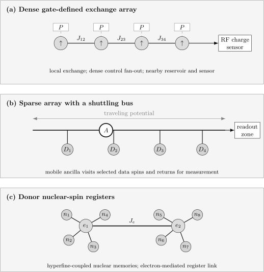
Three distinct architecture contracts. A dense array uses local exchange and nearby sensors; a sparse array moves an ancilla spin between interaction zones; a donor architecture couples nuclear-spin registers through shared electrons. Dot count, physical-spin count, encoded-qubit count, and logical qubit count must be reported separately.
Dense exchange arrays
Section titled “Dense exchange arrays”In a dense array, each dot has plunger and barrier controls and neighboring spins interact through exchange. The layout is compact, but electrodes, reservoirs, sensors, fan-out, and cross-capacitance compete for area. A two-dimensional error-correction layout may require shared gates, multilayer routing, sparse readout zones, or moving information to avoid placing a complete analog control chain beside every dot.
Sparse arrays and shuttling
Section titled “Sparse arrays and shuttling”An alternative is to leave transport channels between storage or interaction sites. Time-dependent gate voltages move an electron through a sequence of dots or a traveling electrostatic minimum. A mobile ancilla can visit several data qubits and then return to a readout zone.
Shuttling changes routing from a sequence of logical SWAP gates into physical motion, but it does not make routing free. One must include
where includes spin dephasing, valley or orbital excitation, charge loss, phase uncertainty, and loading error for transport segment . Static disorder and low-valley-splitting regions become more likely as the traveled distance and number of gates grow.
Donor registers and modular links
Section titled “Donor registers and modular links”A donor register can use one electron to address several nuclear spins, creating dense internal connectivity. Exchange between register electrons then supplies a modular link. The favorable count of control primitives must be weighed against spectral calibration, shared-resource scheduling, atomic placement, and the consequences of losing or mis-tuning one linking electron.
Loading, Tuning, and Virtual Gates
Section titled “Loading, Tuning, and Virtual Gates”Charge stability comes first
Section titled “Charge stability comes first”Before a spin qubit exists operationally, the device must be placed in a known charge configuration. Sweeps of gate voltages and a charge sensor reveal transitions between integer occupations. Tunnel rates to reservoirs and between dots are then adjusted so that initialization and measurement are fast enough while coherent evolution remains isolated.
In a many-gate device, every electrode affects several electrochemical potentials. If is the vector of physical voltages and the vector of dot potentials, a local linear model is
A virtual-gate transformation chooses
where is an inverse or pseudoinverse calibrated near one operating point. This compensates first-order electrostatic crosstalk. It is not a global cure: drifts and becomes nonlinear when barriers, occupations, or reservoir conditions change.
Tuning is a state-estimation problem
Section titled “Tuning is a state-estimation problem”An array is tuned by inferring hidden device parameters from charge-sensor signals, spin resonances, exchange oscillations, and held-out validation sequences. The result is not simply a table of voltages. It is a time-stamped model with uncertainty:
where are tunnel couplings and may denote measurement response parameters. Automated tuning is essential because the number of cross-couplings grows quickly, but automation must report failure rates and validation data rather than only successful examples.
Initialization and Readout
Section titled “Initialization and Readout”Thermal polarization
Section titled “Thermal polarization”If a spin equilibrates at temperature with Zeeman splitting , its ground-state probability is
For an electron with at and , , so . Merely waiting for thermal equilibrium is then inadequate for high-fidelity initialization. Larger fields, lower electron temperatures, energy-selective tunneling, measurement and feedback, algorithmic cooling, or initialization through a larger orbital or charge gap can improve the result.
The relevant is the electronic distribution seen by the dot, not simply the refrigerator thermometer. Reservoir heating, microwave power, filtering, and nonequilibrium tails can dominate rare initialization errors.
Energy-selective tunneling
Section titled “Energy-selective tunneling”Place the electrochemical potential for one spin state above a reservoir Fermi level and the other below it. The unwanted spin can tunnel out and be replaced by the desired state. The same mechanism supports single-shot readout: one spin orientation produces a transient charge event while the other remains trapped.
The assignment fidelity depends on more than sensor signal-to-noise:
- tunnel-out and tunnel-in rates relative to the acquisition window;
- relaxation during the measurement;
- thermal tunneling of the nominally blocked state;
- missed short events because of finite detector bandwidth;
- state preparation before the readout pulse;
- thresholding, filtering, and drift in the charge sensor.
The declared reference plane matters. A spin-to-charge conversion fidelity and a final digital assignment fidelity are different quantities.
Pauli spin blockade
Section titled “Pauli spin blockade”In a double dot, detuning toward a doubly occupied charge state can allow a singlet to move while a triplet is blocked by antisymmetry and the available orbital spectrum. A charge sensor then distinguishes the resulting charge configurations. This is a parity-like measurement only under a declared mapping between spin states and charge outcomes.
Valley or orbital excitations can lift the blockade. Spin relaxation, nonadiabatic ramps, incomplete charge conversion, sensor backaction, and latched-state lifetime all enter the error ledger. “Pauli blockade readout” is therefore a protocol, not an ideal projector supplied by the material.
Charge sensors and radio-frequency reflectometry
Section titled “Charge sensors and radio-frequency reflectometry”A quantum point contact, single-electron transistor, sensor dot, or gate-based dispersive sensor responds to a nearby charge configuration. Embedding the sensor in a resonant circuit can translate its conductance or quantum capacitance into the phase and amplitude of a reflected radio-frequency signal.
Sensors consume footprint, reservoirs, resonators, amplifiers, and bandwidth. Architectures may therefore share sensors, shuttle spins to readout zones, or use cascaded charge motion to bring remote parity information within sensing range. Those strategies trade area for latency and additional conversion errors.
One-Qubit Control
Section titled “One-Qubit Control”ESR and the rotating frame
Section titled “ESR and the rotating frame”For a transverse resonant magnetic drive,
Near resonance and under the rotating-wave approximation,
where . Pulse area sets the rotation angle, phase sets the equatorial axis, and a frame update implements a virtual rotation. Microwave magnetic fields can be delivered by a local line or a shared resonator, but global drive requires frequency selectivity and careful accounting of off-resonant rotations.
Electric-dipole spin resonance
Section titled “Electric-dipole spin resonance”An oscillating gate voltage does not directly flip an ideal spin. Spin–orbit coupling or a transverse magnetic-field gradient converts electrically driven motion into an effective oscillating magnetic field. Micromagnets can provide large gradients and distinct qubit frequencies, enabling fast electrical control. They also make spin frequency sensitive to dot position and charge noise, introduce static gradients during exchange and shuttling, and can complicate magnetic uniformity.
Hole spins can have stronger intrinsic spin–orbit coupling and fast all- electrical control without a micromagnet. The same coupling can enhance electric-noise sensitivity and produce anisotropic, device-dependent two-qubit interactions.
Addressability and simultaneous operation
Section titled “Addressability and simultaneous operation”If neighboring qubits differ in frequency by , a pulse with Rabi rate and duration must balance speed against spectral selectivity. The rough condition suppresses off-resonant excitation, but shaped pulses, composite sequences, and calibrated frame corrections refine this tradeoff.
An isolated randomized-benchmarking result does not establish parallel operation. Simultaneous drives can change detuning, induce Stark shifts, heat reservoirs, saturate electronics, or activate microwave and baseband crosstalk. A scalable control claim should report simultaneous or contextual benchmarks on the intended neighborhood.
Exchange and Entangling Gates
Section titled “Exchange and Entangling Gates”Exchange phase
Section titled “Exchange phase”For two spins with
define the exchange area
The unitary is
Up to a global phase, produces SWAP and produces . With unequal Zeeman splittings, adiabatic or resonantly modulated exchange can instead implement controlled-phase or controlled-rotation primitives. Local phases accumulated during the pulse must be calibrated or tracked.
Why exchange is both useful and difficult
Section titled “Why exchange is both useful and difficult”Exchange can be fast because it comes from wave-function overlap and virtual charge motion. It is usually controlled by barrier or detuning voltages, and often varies approximately exponentially over part of the operating range:
Then a small voltage fluctuation produces
The same electrical leverage that makes a fast gate also amplifies charge noise and waveform distortion. A gate calibrated by exchange oscillations can still fail in a circuit because neighboring pulses, sensor states, or slow drift change the operating point.
Symmetric operation
Section titled “Symmetric operation”For a double dot, let denote detuning and a barrier coordinate. Near a charge-symmetric point,
Detuning noise then enters at second order:
This reduces one noise pathway, not all electrical noise. Barrier noise, cross-capacitance, pulse distortion, nuclear gradients, and leakage remain. A “sweet spot” is always a derivative statement with respect to specified coordinates.
Long-range couplers
Section titled “Long-range couplers”Direct exchange falls rapidly with distance. Proposed and demonstrated extensions include:
- physically shuttling electrons between interaction zones;
- superexchange through intermediate empty or occupied dots;
- capacitive coupling between charge-admixed spin encodings;
- coupling electric dipoles to superconducting microwave resonators;
- donor-register links through exchange-coupled electrons.
Each method changes the error channel. Shuttling risks transport leakage and phase pickup; superexchange introduces virtual-state sensitivity; capacitive and resonator couplings require charge or spin–photon admixture and can expose the spin to electric loss. Connectivity should be quoted with gate time, fidelity, concurrency, idle impact, and required intermediate hardware.
Error and Leakage Ledger
Section titled “Error and Leakage Ledger”Residual nuclear spins
Section titled “Residual nuclear spins”Natural silicon contains spinful . Isotopic enrichment in can strongly reduce the fluctuating Overhauser field, but the residual concentration, spatial distribution, and nearby spinful materials still matter. Si/SiGe stacks may also contain spinful . Slow nuclear fluctuations often appear as qubit-frequency drift or quasi-static dephasing rather than a memoryless phase-flip channel.
Enrichment improves magnetic coherence but does not remove charge noise, valley disorder, control errors, or phonon-mediated relaxation. A long dynamically decoupled must not be used as a substitute for gate or code performance.
Charge noise
Section titled “Charge noise”Charge fluctuators in oxides, interfaces, dielectrics, gates, and reservoirs shift dot potentials and tunnel barriers. They affect:
- exchange amplitudes and conditional phases;
- electric-dipole spin resonance through dot motion;
- Stark-shifted qubit frequencies and factors;
- valley and orbital energies;
- spin-to-charge conversion and sensor thresholds.
Low-frequency noise causes drift and nonexponential Ramsey decay. Noise near gate modulation frequencies causes stochastic gate error. Rare switching events can produce non-Gaussian tails. One spectral-density number cannot replace time-domain stability and contextual circuit tests.
Valley and orbital leakage
Section titled “Valley and orbital leakage”If a control pulse approaches an avoided crossing involving a valley or orbital state, nonadiabatic transitions can populate it. A simple Landau–Zener estimate for an isolated avoided crossing is
where is the minimum gap and is the diabatic energy-sweep rate. Real devices can have multiple crossings, dephasing, and pulse-dependent matrix elements, so the formula is a diagnostic scale rather than a complete leakage model.
Valley leakage can return coherently and masquerade as phase error, remain outside the code space, or alter a later measurement. Benchmarking that assumes a trace-preserving qubit channel can miss it.
Spin relaxation and hot spots
Section titled “Spin relaxation and hot spots”Spin–orbit and hyperfine admixture allow phonons or electrical noise to flip a spin. Near a spin–valley anticrossing, relaxation can be enhanced strongly. therefore depends on field, gate voltages, temperature, valley splitting, and device orientation. It must be measured near the actual operating points, including readout and shuttling configurations.
Leakage in encoded qubits
Section titled “Leakage in encoded qubits”Singlet–triplet and exchange-only qubits use only part of a multi-spin Hilbert space. Control errors can enter polarized triplets or the manifold. Leakage can persist across many cycles and create correlated faults when a leaked spin interacts with neighbors.
A leakage-reduction unit may swap or reset leaked population through an ancilla or reservoir. Its cost includes extra exchange pulses, idle exposure, reset error, and schedule depth. Reporting a low in-subspace gate error while omitting leakage is incomplete.
Drift, context, and correlation
Section titled “Drift, context, and correlation”Qubit frequencies, exchange curves, tunnel rates, and sensor thresholds drift on different timescales. Feedback can keep one parameter locked while moving another. Shared controls and reservoirs can correlate errors spatially; low-frequency drift can correlate them temporally.
Fault-tolerance models need more than average gate infidelity. Useful diagnostics include leakage rates, simultaneous randomized benchmarking, cycle benchmarking, repeated-syndrome correlations, detector-event graphs, and held-out circuit prediction.
Temperature and Cryogenic Architecture
Section titled “Temperature and Cryogenic Architecture”“Hot qubit” is a scoped statement
Section titled ““Hot qubit” is a scoped statement”For an electron with ,
while
Operation above is possible when initialization and readout do not rely solely on thermal Zeeman polarization and when orbital, valley, charging, and reservoir scales remain suitable. A two-qubit demonstration above establishes an important component regime. It does not show that a large processor, its amplifiers, its interconnects, and its fault-tolerant cycle all operate at that temperature.
Where the classical controller lives
Section titled “Where the classical controller lives”Dense spin arrays create a wiring problem even though each qubit is small. Possible partitions include:
- room-temperature waveform generation with filtered lines to the millikelvin stage;
- cryogenic multiplexers or controllers at an intermediate stage near –;
- selected digital or analog electronics at the millikelvin stage;
- shared, crossbar, or globally broadcast controls with local selectivity.
Moving electronics colder reduces cable count and latency but consumes cooling power and can inject electrical or magnetic noise. Moving it warmer requires high-density low-thermal-conductance links with adequate bandwidth and signal integrity. A credible architecture states power per channel, static bias count, update rate, conversion resolution, line heat leak, sensor bandwidth, and feedback latency.
Cryogenic and Vacuum Infrastructure supplies the stage-by-stage heat, wiring, noise, shielding, and diagnostic contract needed to test such a partition.
Fabrication, Yield, and Automated Operation
Section titled “Fabrication, Yield, and Automated Operation”CMOS compatibility is an opportunity, not an identity
Section titled “CMOS compatibility is an opportunity, not an identity”Silicon spin devices can use industrial materials, lithography, gate stacks, vias, and wafer-scale metrology. However, a transistor process optimized for classical threshold voltage, mobility, and leakage is not automatically optimized for few-electron disorder, valley splitting, charge noise, and coherent exchange.
Foundry evidence should be separated into:
- geometric yield and dimensional variation;
- ability to accumulate and isolate single electrons;
- charge-noise and valley-splitting distributions;
- qubit coherence and gate performance across devices;
- simultaneous operation of a connected array;
- back-end routing, packaging, and cryogenic-controller integration.
Success at one level is valuable without proving the next.
Variability consumes control resources
Section titled “Variability consumes control resources”Suppose device parameters have a distribution with mean and spread . A controller can compensate some variation by per-qubit biases and pulse parameters, but each compensation consumes memory, calibration time, voltage range, and crosstalk margin. Fabrication uniformity and control sophistication are therefore interchangeable only within limits.
Yield also compounds. If a required unit cell succeeds independently with probability , an unrepairable array of cells succeeds with probability
Independence is rarely exact, but the formula shows why spare cells, rerouting, defect maps, and repairable architectures matter even when is high.
Tuning time belongs in the runtime ledger
Section titled “Tuning time belongs in the runtime ledger”A processor with fast nanosecond exchange pulses can still have slow availability if loading, mapping charge transitions, fitting crosstalk, locking frequencies, and validating gates require extensive intervention. Operational metrics should include:
The relevant fraction is useful experimental time divided by total scheduled time, with failures and retuning included.
Processor Metrics
Section titled “Processor Metrics”The generic definitions in Metrics for Quantum Hardware apply, but silicon spin processors need several additional labels.
| Quantity | Ambiguity to remove |
|---|---|
| dot count | Does every dot contain a controlled spin? Are some dots buses, sensors, reservoirs, or leakage sinks? |
| physical-spin count | Are electrons, nuclei, readout ancillas, and mobile ancillas all included? |
| encoded-qubit count | Does one qubit consume one, two, or three spins? |
| connected count | Which pairs have calibrated entangling operations in the same configuration? |
| active count | Which qubits are initialized, controlled, and measured in one experiment? |
| logical count | Is the code detecting or correcting errors, and are logical gates protected? |
For an exchange gate, report pulse duration, exchange area, leakage, single-qubit phase corrections, spectator conditions, and benchmark protocol. For readout, report spin-to-charge conversion, sensor assignment, integration time, relaxation correction, and whether assignment is simultaneous. For shuttling, report distance, time, number of segments, state fidelity, phase calibration, charge-survival probability, and the extrapolation model.
A minimal code-cycle time is
Fast exchange alone may be a small part of this sum.
Fault Tolerance and Logical Evidence
Section titled “Fault Tolerance and Logical Evidence”Component thresholds are conditional
Section titled “Component thresholds are conditional”A physical gate fidelity above a quoted surface-code threshold is encouraging only after matching the assumed noise model, leakage treatment, connectivity, measurement schedule, and simultaneous-operation conditions. There is no platform-independent rule that “above ” means fault tolerant.
The stronger experiment repeats syndrome extraction, decodes the record, and tests whether logical error falls when code distance or another protection resource increases under comparable conditions.
What early correction experiments established
Section titled “What early correction experiments established”A 2022 three-spin silicon experiment encoded one data qubit against phase flips and used a coherent iToffoli correction. The corrected response suppressed first-order sensitivity to injected single-qubit phase errors and mitigated quasi-static dephasing. It did not perform repeated, measurement-based syndrome extraction, and its corrected fidelity remained limited by the correction circuitry. This was a code-primitive demonstration, not a scalable logical memory.
Error detection is not error correction
Section titled “Error detection is not error correction”The code encodes two logical qubits and detects any single-qubit Pauli error, but distance two cannot identify and correct an arbitrary single-qubit error without additional information. Postselecting on a clean syndrome can raise conditional fidelity while lowering throughput:
Both quantities must be reported. A universal set of operations on encoded states is a major control result, but it does not by itself demonstrate that logical error decreases with code distance or that operations are fault-tolerant under repeated correction.
Weight-four parity checks
Section titled “Weight-four parity checks”A surface-code stabilizer requires one ancilla to interact with several data qubits and then be measured without destroying the data. Demonstrating -type and -type parity checks up to weight four in a shuttling architecture tests this connectivity and measurement primitive. One five-qubit plaquette does not yet establish a repeated two-dimensional surface-code memory, decoder performance, or scaling below threshold.
Repetition-code scaling
Section titled “Repetition-code scaling”A distance-5 repetition code tests one classical error type and can reveal correlated faults over many rounds. In July 2026, an exchange-only silicon system reported a logical error rate near for a distance-5 experiment, compared with about for average distance-3 subsets extracted from the same data. That suppression is genuine code-scaling evidence for the tested repetition-code setting.
It is not a full quantum memory because a one-basis repetition code does not protect arbitrary quantum information against both bit and phase errors. In the same work, a postselected experiment reached a conditional two-logical-qubit state fidelity near after three syndrome rounds while rejecting roughly of shots. The acceptance cost is part of the result.
Evidence Through August 2026
Section titled “Evidence Through August 2026”Hardware records are date-sensitive. The entries below are selected because they test different layers of the architecture rather than because they can be combined into one imaginary best device.
| Date and experiment | What was established | What was not established by that result |
|---|---|---|
| 2022, high-fidelity two-qubit devices | Several silicon implementations reported one- and two-qubit gate benchmarks above under specified protocols. | A common error model, simultaneous large-array performance, or a complete code cycle. |
| 2022, six-dot processor | Universal control, calibration, entanglement, and algorithmic circuits were demonstrated across six gate-defined electron spins. | A six-logical-qubit processor or scalable fault tolerance. |
| 2022, three-spin phase correction | A coherent phase-flip code reduced first-order sensitivity to injected errors. | Repeated syndrome measurement or below-threshold logical scaling. |
| 2024, operation above | A two-qubit SiMOS device combined algorithmic initialization, readout, and universal control above . | A large processor or its complete classical stack operating at that temperature. |
| 2024–2026, 300-mm processing | Wafer-scale studies probed single-electron devices, foundry-made two-qubit cells exceeded control fidelity, and an eight-dot foundry array was coherently characterized. | Uniform high-fidelity operation of a large two-dimensional processor; the eight-dot study read the central four and demonstrated a two-qubit gate on a pair. |
| 2025, conveyor shuttling | A spin was transported over a cumulative in under with a reported shuttling fidelity for the benchmarked operation. | A repeated error-correction route across a full processor or unchanged fidelity over arbitrary distance. |
| 2025, donor registers | Two exchange-linked donor registers formed an 11-spin processor with nine nuclear data spins and two electrons; local and nonlocal entanglement were demonstrated with high control fidelities. | A foundry-style gate-defined array or a large error-corrected logical register. |
| March 2026, donor logical processor | A five-nuclear-spin donor system implemented the encoding, fault-tolerant state preparation under the paper’s criteria, and a characterized universal logical gate set. | Distance scaling, arbitrary single-error correction, or a long-running fault-tolerant computation. |
| July 2026, shuttling plaquette | A mobile ancilla connected four data spins, enabling universal control, weight-four parity checks, and five-spin GHZ entanglement. | Repeated operation of a two-dimensional surface-code patch below threshold. |
| July 2026, integrated exchange-only system | A 54-dot chip configurable for up to 18 exchange-only qubits was integrated with a digital controller and a superconducting interconnect; seven- and six-qubit code experiments tested repeated operation. | Eighteen simultaneously validated logical qubits or a universal fault-tolerant processor. |
The trend is substantial: the field has moved from isolated spin control to foundry reproducibility, integrated control, transport-based connectivity, multi-register operation, parity checks, and small encoded circuits. The remaining gap is also substantial: no silicon-spin experiment has yet shown a universal large-distance code with sustained logical suppression under a complete, scalable cycle.
Advantages and Bottlenecks
Section titled “Advantages and Bottlenecks”Architectural advantages
Section titled “Architectural advantages”- Small carrier footprint. Dot pitches can be far below those of many atomic or superconducting layouts, leaving room in principle for dense coding.
- Long-lived spin degrees of freedom. Isotopic enrichment can strongly suppress one major magnetic bath.
- Fast local exchange. Baseband electrical pulses can implement local entangling operations without a separate optical system.
- Semiconductor process leverage. Wafer metrology, multilayer routing, device models, and cryogenic CMOS can be adapted rather than invented from nothing.
- Several useful encodings. One-spin, decoherence-reduced, exchange-only, and electron–nuclear register designs permit architecture–noise co-design.
- Movable carriers. Physical shuttling can create dynamic connectivity and centralized readout.
Central bottlenecks
Section titled “Central bottlenecks”- Electrostatic complexity. Many gates control coupled, nonlinear potentials; tuning and drift grow with array size.
- Interface and valley variability. Atomic-scale disorder changes leakage gaps and exchange.
- Local interaction geometry. Direct exchange is short range, so routing and syndrome scheduling are first-class costs.
- Readout footprint and latency. Reservoirs, sensors, resonators, and amplifiers do not shrink with the spin wave function.
- Charge sensitivity during useful operations. Exchange and electrical spin control deliberately admix charge or motion.
- Leakage. Valley, orbital, charge, polarized-triplet, and total-spin sectors can retain errors outside a qubit-only model.
- Cryogenic fan-out. Density moves the problem into wiring, heat, controller power, and signal integrity.
- Evidence transfer. Best coherence, gate, temperature, fabrication, shuttling, and logical results come from different devices and encodings.
No one scalar ranks these tradeoffs. The useful comparison is a compiled workload or repeated code cycle with every physical and classical resource included.
Worked Audit: “An 18-Qubit Fault-Tolerant Silicon QPU”
Section titled “Worked Audit: “An 18-Qubit Fault-Tolerant Silicon QPU””Consider the statement:
A digitally controlled silicon QPU contains 18 qubits and demonstrates fault-tolerant quantum computing.
The first clause needs a count definition. The 2026 system used a 54-dot three-rail device configurable for up to 18 three-spin exchange-only qubits. That is a hardware capacity statement. The reported code experiments used smaller active subsets: seven encoded qubits for a distance-5 repetition code and six for a error-detection experiment.
The second clause overstates the evidence. What the experiment established includes:
- integrated digital control of millikelvin qubits through a high-density low-thermal-conductance interconnect;
- multi-qubit exchange-only control with dynamical decoupling and leakage-reduction operations;
- repeated distance-5 repetition-code cycles with improved logical error relative to distance-3 subsets;
- three rounds of error detection with a reported conditional logical-state fidelity and acceptance fraction;
- agreement between measured code data and calibrated simulations at the reported scale.
It did not establish:
- arbitrary quantum-error correction by the repetition code;
- a distance-scaled universal logical gate set;
- an 18-logical-qubit computation;
- acceptable power, yield, calibration, and routing at utility scale.
A defensible summary is:
An integrated silicon exchange-only QPU demonstrated cryogenic digital control and repeated small-code experiments, including distance-dependent suppression for a one-basis repetition code and postselected quantum error detection.
That wording is still a strong result. Precision does not diminish it.
A Practical Comparison Checklist
Section titled “A Practical Comparison Checklist”When reading or designing a silicon-spin experiment, record:
- material stack, isotope concentrations, dot or donor process, and device temperature;
- physical carrier, charge state, code space, and nearby leakage states;
- magnetic field, valley and orbital gaps, reservoir conditions, and relevant tunnel rates;
- one-qubit and two-qubit control mechanisms, pulse durations, and simultaneous spectators;
- initialization and readout reference planes, integration windows, and assignment model;
- calibrated connectivity, routing operations, shuttling distances, and required phase tracking;
- , Ramsey , echo or decoupled , charge-noise diagnostics, and leakage;
- calibration frequency, tune-up success rate, drift response, and useful uptime;
- controller location, channel count, power, heat load, bandwidth, and feedback latency;
- physical, encoded, active, and logical qubit counts;
- benchmark protocol, uncertainty, accepted-event fraction, and excluded costs;
- whether the claim concerns a component, processor, code primitive, logical memory, logical gate, or workload.
Common Mistakes
Section titled “Common Mistakes”- Treating “spin” as electrically isolated even though initialization, exchange, EDSR, shuttling, and readout use charge motion.
- Calling every confined electron a controlled qubit.
- Equating dot count, spin count, exchange-only encoded count, and logical qubit count.
- Assuming isotopic enrichment removes all important noise.
- Ignoring valley states because the intended qubit basis contains only spin.
- Quoting an isolated gate fidelity as a simultaneous code-cycle error.
- Treating a sweet spot in detuning as immunity to barrier and common-mode voltage noise.
- Calling coherent shuttling equivalent to a perfect long-range gate.
- Combining a foundry yield from one process, a gate record from another, and a logical result from a third into one projected machine without an interface model.
- Treating operation above as proof that the entire computer can run at .
- Calling a distance-2 error-detecting code an arbitrary-error-correcting memory.
- Calling one weight-four stabilizer measurement a surface-code computer.
- Omitting postselection loss when reporting conditional logical fidelity.
- Treating CMOS compatibility as already-completed co-integration.
Exercises
Section titled “Exercises”1. Thermal polarization
Section titled “1. Thermal polarization”Take an electron with at . Estimate its ground-state thermal population at and . Use and . Explain why a hot-qubit experiment may require algorithmic initialization.
Solution
The Zeeman splitting is
At ,
so
At ,
and
Thermal waiting at therefore leaves roughly one spin in five excited in this ideal two-level estimate. Measurement, feedback, entropy transfer, or energy-selective loading is needed for high-purity initialization.
2. Exchange pulse area
Section titled “2. Exchange pulse area”Two spins have a constant exchange frequency . Neglect all Zeeman gradients and pulse ramps. Find the duration of a pulse.
Solution
The exchange area is
For , , so
A real pulse needs ramp corrections, single-qubit phase tracking, and a leakage check.
3. Charge-noise leverage
Section titled “3. Charge-noise leverage”Assume with . Estimate the fractional exchange error caused by a quasi-static voltage offset of . What phase error does this produce for an otherwise ideal pulse?
Solution
To first order,
For fixed duration, the exchange area has the same fractional error:
This is only the quasi-static contribution from the chosen voltage coordinate. Broadband noise and pulse distortion require a filter-function or full control model.
4. A two-dot virtual gate
Section titled “4. A two-dot virtual gate”Near one operating point, suppose
Find physical voltage changes that shift only dot 1 by .
Solution
The determinant is . Inverting the matrix gives
Therefore
The compensating change on gate 2 cancels its first-order influence on . The calibration remains local and must be updated if the cross-capacitance matrix changes.
5. Compound shuttling fidelity
Section titled “5. Compound shuttling fidelity”A simplified model assigns an independent fidelity to each gate-pitch transport segment. Estimate the survival of the intended spin state after 250 segments. State two reasons this extrapolation may fail.
Solution
Under the independent identical-error model,
The approximation can fail because phase errors may be coherent and add systematically rather than independently. It can also fail because different locations have different disorder and valley gaps. Charge loss, common waveform errors, and drift provide further violations.
6. Readout is a response matrix
Section titled “6. Readout is a response matrix”Let be the probability of declaring down when the spin is down, and the probability of declaring up when it is up. For an equal prior mixture, find the probability of an up declaration and the posterior probability that the spin was actually up given that declaration.
Solution
The up-declaration probability is
Bayes’ rule gives
Assignment fidelity and posterior confidence depend on different conditionals; the latter also depends on the input prior.
7. Yield compounding
Section titled “7. Yield compounding”An unrepairable design needs 1,000 statistically independent unit cells. If each has yield , what is the complete-array yield? What architecture lesson follows?
Solution
The idealized array yield is
A seemingly high cell yield leaves only about perfect arrays at this size. Larger systems need better yield, spare cells, defect-aware mapping, repair, or routing around failures. Correlated wafer defects can make the independent model optimistic or pessimistic, so measured spatial statistics are required.
8. Count the qubits
Section titled “8. Count the qubits”A chip has 54 quantum dots arranged so that each exchange-only encoded qubit uses three spins. Seven encoded qubits are active in one repetition-code experiment, five of them serving as data and two as syndrome ancillas. Give the dot-capacity count, encoded-capacity count, active encoded count, and logical count for that experiment.
Solution
The chip has 54 dots and a nominal capacity of
exchange-only encoded qubits, assuming every required trio is loaded and usable. The experiment actively uses seven encoded qubits. The repetition code encodes one classical logical bit against one error type in five data qubits, with two ancillas. It should not be reported as one arbitrary quantum logical qubit protected against both and errors.
9. Classify a logical claim
Section titled “9. Classify a logical claim”A experiment prepares encoded states, runs logical gates, rejects shots with nontrivial syndromes, and reports higher fidelity on accepted shots. What has been demonstrated, and what two quantities are required to interpret the result?
Solution
The experiment demonstrates encoded state preparation, logical control, and single-error detection in the tested circuits. It may also demonstrate fault-tolerant construction of selected operations under explicit fault-propagation criteria.
It does not demonstrate arbitrary single-error correction or distance scaling because the code has distance two. At minimum one must report both the conditional logical fidelity and the acceptance probability or accepted throughput. Otherwise postselection can make the retained sample look better while discarding most attempts.
10. Design a routing comparison
Section titled “10. Design a routing comparison”Compare two ways to connect distant data spins: a sequence of nearest-neighbor SWAP gates and physical electron shuttling. List the minimum measurements needed for a fair experiment.
Solution
For both routes, measure total time, final state or process fidelity, leakage, charge survival, phase error, spectator disturbance, and calibration stability over the same distance and initial-state ensemble.
The SWAP route additionally needs the number and fidelity of compiled exchange gates, idle errors, and whether logical mapping is restored. The shuttling route needs the physical path, segment or cycle count, transport waveform, charge-loss probability, valley or orbital excitation, accumulated phase, and return/readout overhead. Both comparisons must include concurrent operations and the controls required to maintain the route.
References
Section titled “References”- D. Loss and D. P. DiVincenzo, “Quantum computation with quantum dots,” Physical Review A 57, 120–126 (1998), doi:10.1103/PhysRevA.57.120.
- B. E. Kane, “A silicon-based nuclear spin quantum computer,” Nature 393, 133–137 (1998), doi:10.1038/30156.
- F. A. Zwanenburg et al., “Silicon quantum electronics,” Reviews of Modern Physics 85, 961–1019 (2013), doi:10.1103/RevModPhys.85.961.
- G. Burkard, T. D. Ladd, A. Pan, J. M. Nichol, and J. R. Petta, “Semiconductor spin qubits,” Reviews of Modern Physics 95, 025003 (2023), doi:10.1103/RevModPhys.95.025003.
- P. Stano and D. Loss, “Review of performance metrics of spin qubits in gated semiconducting nanostructures,” Nature Reviews Physics 4, 672–688 (2022), doi:10.1038/s42254-022-00484-w.
- R. Hanson, L. P. Kouwenhoven, J. R. Petta, S. Tarucha, and L. M. K. Vandersypen, “Spins in few-electron quantum dots,” Reviews of Modern Physics 79, 1217–1265 (2007), doi:10.1103/RevModPhys.79.1217.
- J. M. Elzerman et al., “Single-shot read-out of an individual electron spin in a quantum dot,” Nature 430, 431–435 (2004), doi:10.1038/nature02693.
- A. Morello et al., “Single-shot readout of an electron spin in silicon,” Nature 467, 687–691 (2010), doi:10.1038/nature09392.
- J. J. Pla et al., “A single-atom electron spin qubit in silicon,” Nature 489, 541–545 (2012), doi:10.1038/nature11449.
- M. Veldhorst et al., “A two-qubit logic gate in silicon,” Nature 526, 410–414 (2015), doi:10.1038/nature15263.
- J. Yoneda et al., “A quantum-dot spin qubit with coherence limited by charge noise and fidelity higher than ,” Nature Nanotechnology 13, 102–106 (2018), doi:10.1038/s41565-017-0014-x.
- A. Noiri et al., “Fast universal quantum gate above the fault-tolerance threshold in silicon,” Nature 601, 338–342 (2022), doi:10.1038/s41586-021-04182-y.
- X. Xue et al., “Quantum logic with spin qubits crossing the surface code threshold,” Nature 601, 343–347 (2022), doi:10.1038/s41586-021-04273-w.
- M. T. Mądzik et al., “Precision tomography of a three-qubit donor quantum processor in silicon,” Nature 601, 348–353 (2022), doi:10.1038/s41586-021-04292-7.
- A. R. Mills et al., “Two-qubit silicon quantum processor with operation fidelity exceeding ,” Science Advances 8, eabn5130 (2022), doi:10.1126/sciadv.abn5130.
- K. Takeda et al., “Quantum error correction with silicon spin qubits,” Nature 608, 682–686 (2022), doi:10.1038/s41586-022-04986-6.
- S. G. J. Philips et al., “Universal control of a six-qubit quantum processor in silicon,” Nature 609, 919–924 (2022), doi:10.1038/s41586-022-05117-x.
- A. J. Weinstein et al., “Universal logic with encoded spin qubits in silicon,” Nature 615, 817–822 (2023), doi:10.1038/s41586-023-05777-3.
- J. Y. Huang et al., “High-fidelity spin qubit operation and algorithmic initialization above ,” Nature 627, 772–777 (2024), doi:10.1038/s41586-024-07160-2.
- S. Neyens et al., “Probing single electrons across 300-mm spin qubit wafers,” Nature 629, 80–85 (2024), doi:10.1038/s41586-024-07275-6.
- T. Tanttu et al., “Assessment of the errors of high-fidelity two-qubit gates in silicon quantum dots,” Nature Physics 20, 1804–1809 (2024), doi:10.1038/s41567-024-02614-w.
- P. Steinacker et al., “Industry-compatible silicon spin-qubit unit cells exceeding fidelity,” Nature 646, 81–87 (2025), doi:10.1038/s41586-025-09531-9.
- M. De Smet et al., “High-fidelity single-spin shuttling in silicon,” Nature Nanotechnology 20, 866–872 (2025), doi:10.1038/s41565-025-01920-5.
- S. K. Bartee et al., “Spin-qubit control with a milli-kelvin CMOS chip,” Nature 643, 382–387 (2025), doi:10.1038/s41586-025-09157-x.
- H. Edlbauer et al., “An 11-qubit atom processor in silicon,” Nature 648, 569–575 (2025), doi:10.1038/s41586-025-09827-w.
- C. Zhang et al., “Universal logical operations in a silicon quantum processor,” Nature Nanotechnology 21, 635–641 (2026), doi:10.1038/s41565-026-02140-1.
- T. Tanttu et al., “Eight-qubit operation of a 300 mm SiMOS foundry-fabricated device,” Nature Communications 17, 5878 (2026), doi:10.1038/s41467-026-74597-6.
- B. Undseth et al., “Weight-four parity checks in a spin-shuttling architecture,” Nature 655, 1160–1166 (2026), doi:10.1038/s41586-026-10766-3.
- Members of the HRL Quantum Team and Collaborators, “A digitally controlled silicon quantum processing unit,” Nature 655, 1154–1159 (2026), doi:10.1038/s41586-026-10754-7.
Further Connections
Section titled “Further Connections”- Hardware Overview gives the platform-neutral comparison contract.
- Control, Readout, and Calibration develops the closed-loop operating system used here.
- Cryogenic and Vacuum Infrastructure develops the thermal-stage, wiring, shielding, noise, and availability ledger for the refrigerator and its classical interfaces.
- Materials and Fabrication Interface connects isotope purity, oxides, gate stacks, wafer distributions, shared operating windows, screening, calibration burden, and array yield.
- Quantum Dots owns confinement, addition energies, and valley-aware device physics.
- Coulomb Blockade and Mesoscopic Transport own reservoir and charge-transition models.
- Spin Qubits owns relaxation, dephasing, spectra, dynamical decoupling, and measurement backaction.
- Exchange Interactions supplies the microscopic bridge to effective exchange gates.
- Why Quantum Error Correction Is Possible and Surface Code provide the code criteria behind the evidence labels.