Defect and Solid-State Spin Qubits
An optically addressable spin defect is an atom-scale quantum system embedded in a macroscopic crystal. Its localized electronic levels can supply a controllable spin, its optical transition can connect that spin to a photon, and nearby nuclear spins can supply longer-lived storage. The same ingredients support three rather different technologies: a local sensor, a small hybrid processor, or a node in a photonic quantum network.
That compactness is the platform’s central opportunity and its central difficulty. The host is not an inert package. Isotopes, strain, surfaces, implantation damage, charge traps, phonons, and nanophotonic fabrication all enter the operational quantum model. A statement such as “the defect has a one-second coherence time” says little about a network unless it also states which spin, pulse sequence, optical activity, temperature, and device geometry produced that number.
Purpose and Canonical Scope
Section titled “Purpose and Canonical Scope”This page owns the hardware and architecture layer for optically addressable solid-state spins. It develops:
- the physical degrees of freedom and encoding choices;
- electron–nuclear register architectures;
- optical interfaces, cavities, collection, and telecom conversion;
- initialization, coherent control, readout, and local gates;
- heralded links, memory-under-network-activity, and real-time feed-forward;
- material, fabrication, yield, and scaling constraints;
- the evidence boundary between demonstrated components and scalable systems.
NV Centers and Solid-State Defects is the canonical home for optical pumping, fluorescence backaction, relaxation, dephasing, and defect-based sensing in open-system language. NV-Center Sensing owns end-to-end NV sensing protocols, photon likelihoods, spatial transfer, nanoscale NMR, and evidence. Magnetometry owns the platform-neutral metrology framework. This article uses those results but does not repeat their derivations.
The phrase solid-state spin qubit is broader than color center. Here the main families are vacancy complexes and impurities with coherent optical interfaces: nitrogen-vacancy (NV) and group-IV vacancy centers in diamond, divacancies and silicon vacancies in silicon carbide, optically active defects such as the T center in silicon, and selected rare-earth ions in crystals. Gate-defined semiconductor dots and donor processors instead live in Silicon Spin Qubits.
The Architecture Contract
Section titled “The Architecture Contract”A defect platform is not specified by naming a defect species. Write for its operational specification. A complete architecture statement should identify at least:
- host and defect configuration;
- charge state and spin manifold;
- communication and memory encodings;
- optical transition and photonic structure;
- initialization, gates, and readout;
- temperature and magnetic-field regime;
- link protocol and detector model;
- fabrication, tuning, and calibration stack.
Two devices with the same chemical defect can implement different hardware. One room-temperature NV center under off-resonant green excitation may be a nanoscale magnetometer. Another NV center at a few kelvin, driven on resolved optical transitions and coupled to a nuclear memory, may be a network node. Their state preparation, readout, dominant noise, photon budget, and useful metrics are different.
Three qubit counts must also remain separate:
- Spectroscopically observed spins are distinguishable resonances or mapped couplings.
- Controllable register qubits can be initialized, gated, and measured with a declared fidelity and crosstalk model.
- Logical or network qubits satisfy an encoding or distributed protocol with all required operations included.
Mapping a bath of fifty nuclear spins is a remarkable characterization result; it is not, by itself, a fifty-qubit processor.
From a Crystal Defect to a Qubit
Section titled “From a Crystal Defect to a Qubit”Localized levels in a band gap
Section titled “Localized levels in a band gap”A point defect changes the crystal potential and can create localized electronic states inside the host band gap. Occupying those states with a particular number of electrons defines a charge state. Crystal-field and spin–orbit interactions then split orbital and spin multiplets. An optical transition between localized configurations makes the defect a color center when it absorbs or emits within the relevant spectral range.
The useful level structure is therefore conditional on more than chemical identity. It depends on charge state, local strain, electric field, isotope, crystallographic orientation, and sometimes magnetic field. Optical illumination can change the charge state, so ionization and charge recovery belong in the state machine rather than in a footnote.
For a spin- ground manifold, a common effective Hamiltonian is
and describe axial and transverse zero-field splittings, while is the hyperfine tensor for nuclear spin . This is an effective Hamiltonian within a chosen manifold. Optical excitation may change all of these parameters, and group-IV vacancy centers require explicit orbital and spin–orbit degrees of freedom when their orbital branches are not safely eliminated.
Zero-phonon light and phonon sidebands
Section titled “Zero-phonon light and phonon sidebands”An optical excitation can return without changing the vibrational state or can create phonons. The former contributes to the zero-phonon line (ZPL); the latter produces a phonon sideband. Define the Debye–Waller fraction by
where the rates refer to the specified transition and environment. Coherent remote interference generally uses ZPL photons, so a small is a direct efficiency cost unless a cavity selectively enhances the useful channel. NV centers offer excellent spin coherence and mature control, but only a few percent of their free-space emission is in the ZPL. Several group-IV centers direct a substantially larger fraction into their ZPL and have inversion-symmetric structures that reduce first-order sensitivity to some electric-field fluctuations.
The trade is not free. Orbital branches can couple strongly to acoustic phonons, shortening spin coherence unless temperature, strain, or dressed-state control suppresses the process. “Better optical emitter” and “better memory” are separate claims.
Interface spins and memory spins
Section titled “Interface spins and memory spins”The localized electron spin is usually the fastest and most optically visible degree of freedom. A nearby host or impurity nucleus is slower but can remain coherent while the electron is manipulated or repeatedly reset. A useful node therefore assigns roles:
| Physical degree of freedom | Typical role | Strength | Recurring cost |
|---|---|---|---|
| defect electron spin | communication qubit, ancilla, local sensor | fast microwave control and optical access | optical reset, charge noise, shorter memory under activity |
| intrinsic defect nucleus | local memory or flag | deterministic coupling and known identity | isotope availability and fixed hyperfine structure |
| nearby host nucleus | data or memory qubit | potentially long storage and several qubits per defect | device-specific coupling graph and slow gates |
| emitted photon | flying qubit or herald | long-distance transport | loss, indistinguishability, collection, detection |
| orbital or charge state | optical interface, auxiliary, or readout handle | strong coupling to light or electronics | leakage, ionization, phonon sensitivity |
Calling every row a qubit without stating its role obscures the architecture. The photon is not a resident register qubit, and a nuclear memory may be usable only through the electron ancilla.
Representative Platform Families
Section titled “Representative Platform Families”Nitrogen-vacancy centers in diamond
Section titled “Nitrogen-vacancy centers in diamond”The negatively charged NV center has an electronic spin-triplet ground state. At low magnetic field its axial zero-field splitting is approximately . A qubit commonly uses and one of the levels. Microwaves drive the electron spin, optical pumping initializes it, and spin-dependent fluorescence or resonant optical cycling provides readout.
The electron couples to the native nitrogen nucleus and to nearby nuclei. This creates a hub-and-spoke register: the electron is the optically accessible ancilla or communication qubit, while selected nuclei are data, memory, or flag qubits. Dynamical-decoupling sequences on the electron can both protect coherence and synthesize conditional nuclear rotations. Direct radio-frequency driving expands the accessible coupling range but adds timing and calibration demands.
NV centers support room-temperature coherent control and sensing. The high-fidelity resonant optical operations used for single-shot readout and remote entanglement normally require cryogenic operation. Room-temperature spin control therefore does not imply a room-temperature network node.
Group-IV vacancy centers in diamond
Section titled “Group-IV vacancy centers in diamond”Silicon-, germanium-, and tin-vacancy centers place a group-IV impurity between two vacant lattice sites. Their approximate inversion symmetry suppresses a leading electric-dipole response to uniform electric fields and can yield stable, narrow optical transitions. Their spin- ground manifolds and large coherent-emission fractions are attractive for nanophotonic interfaces.
For SiV centers, phonon-driven transitions between orbital branches can limit spin coherence at ordinary cryogenic temperatures. Millikelvin operation, large strain, or continuous dressing can reduce that channel. Heavier group-IV centers have larger orbital splittings and may relax the temperature demand, but fabrication yield, spectral uniformity, charge stability, and complete node demonstrations remain species- and device-dependent.
An isotopically selected center contains a spinful silicon nucleus as a built-in memory. A center similarly supplies an electronuclear register. These deterministic nuclei avoid searching for a particular nearby host isotope, although additional host nuclei can still extend the register.
Defects in silicon carbide
Section titled “Defects in silicon carbide”Silicon carbide combines a wide-band-gap host with mature wafer processing, multiple polytypes, and several optically addressable defect families. Neutral divacancies often have spin- ground states, while negatively charged silicon vacancies can provide spin- manifolds. The latter can be used as a qudit or restricted to a two-level subspace, in which case spectator transitions and leakage must be measured explicitly.
Important demonstrations include coherent control of single defects, spin-to-charge readout, multi-second dynamically decoupled coherence in an isotopically purified device, spin–photon entanglement, and electron–nuclear registers integrated into silicon-carbide-on-insulator waveguides. The host’s industrial maturity is an architectural advantage, not proof that quantum-grade emitters can already be manufactured with uniform yield.
T centers and rare-earth ions
Section titled “T centers and rare-earth ions”The silicon T center is an optically active defect with a telecom O-band transition and an electron spin. A 2026 experiment integrated a T center into a silicon photonic waveguide and controlled a three-qubit register consisting of the electron, a hydrogen nucleus, and a silicon nucleus. This is distinct from a gate-defined silicon dot or a phosphorus donor processor: the optical defect interface is the reason it belongs in this architecture family.
Rare-earth ions such as in crystalline hosts are substitutional impurities rather than vacancy complexes, but they solve the same node problem: a localized spin, narrow optical transitions, and nanophotonic coupling. Their inhomogeneous spectrum can be a burden for matching emitters and a resource for frequency multiplexing. A 2025 two-node experiment used several spectrally distinguishable ytterbium ions to demonstrate remote-pair multiplexing and a three-ion state.
Other emitters, including defects in hexagonal boron nitride, are important research directions. Their inclusion in a platform comparison should follow demonstrated charge-state control, reproducible spin assignment, coherent control, and a quantified optical interface, not brightness alone.
Three Operational Contracts
Section titled “Three Operational Contracts”A sensor
Section titled “A sensor”A sensor uses the electron spin to accumulate a signal-dependent phase or relaxation probability. Spatial resolution, contrast, collection rate, surface distance, and calibration matter alongside coherence. A nearby spin bath may be the signal rather than an error. This contract is developed in NV Centers and Solid-State Defects and Magnetometry.
A local hybrid register
Section titled “A local hybrid register”A register uses the electron as a controllable bus between nuclear memories. The control system must identify the coupling tensor of each chosen nucleus, compile conditional gates, protect spectators, and map nuclear states back to the electron for readout. Its capacity is therefore set by addressability and gate quality, not by the number of spins physically present.
A quantum-network node
Section titled “A quantum-network node”A network node adds an optical interface, low-loss collection, photon filtering, frequency or phase stabilization, detectors, synchronization, and real-time logic. The communication spin is repeatedly optically reset while a nuclear memory stores earlier entanglement. Memory coherence must therefore be measured during network activity, not only while the optical interface is idle.
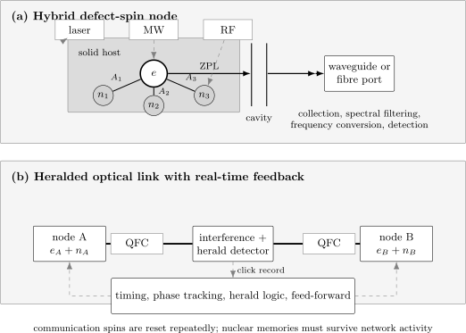
A defect node separates the optically active electron interface spin from nearby nuclear memories . A cavity or waveguide improves useful photon collection; frequency conversion, interference, herald detection, phase tracking, and feed-forward complete a remote link. The nuclear memory must retain coherence while the electron is repeatedly excited and reset.
The three contracts can share a physical defect yet need different figures of merit. Optimizing shallow implantation for sensing can worsen spectral diffusion. Etching a nanocavity can improve collection while degrading spin or optical coherence. An ensemble optimized for magnetic-field sensitivity does not automatically provide individually addressable network nodes.
Initialization and Readout
Section titled “Initialization and Readout”Optical pumping and resonant cycling
Section titled “Optical pumping and resonant cycling”Spin-selective nonradiative decay can polarize a defect into a preferred spin state. Under resonant cryogenic excitation, resolved spin-conserving transitions can instead support repeated cycling and high-fidelity single-shot readout. Both mechanisms are dissipative. The laser changes the spin and can also change the charge state.
The full readout record may include phonon-sideband fluorescence, resonant reflection, arrival times, a charge-state signal, or a repeated mapping from a nucleus to the electron. A quoted assignment fidelity should state whether it is raw, corrected for preparation, conditioned on a charge check, or postselected on consistent repetitions.
For a binary result, report the response matrix
not only its average diagonal. Readout asymmetry matters when a measurement outcome controls feed-forward.
Spin-to-charge and nuclear-assisted readout
Section titled “Spin-to-charge and nuclear-assisted readout”Spin-to-charge conversion maps spin information onto a longer-lived charge configuration and then reads that charge optically or electrically. Repetitive nuclear-assisted readout maps the same memory state to the electron several times. Both can improve signal-to-noise ratio, but each added cycle creates opportunities for memory flips, ionization, and false heralds.
Initialization has the same accounting. A nuclear state may be prepared by measurement and feedback, by polarization transfer from the electron, or by selective optical pumping. A heralded preparation probability must not be reported as deterministic initialization fidelity.
Coherent Control and Local Gates
Section titled “Coherent Control and Local Gates”Electron-spin rotations
Section titled “Electron-spin rotations”Microwave magnetic fields drive electron-spin resonance. In a rotating frame, a selected two-level transition has the familiar control Hamiltonian
The two-level approximation must include leakage to unused spin or orbital levels, off-resonant nuclear-conditioned transitions, pulse distortion, and heating. A fast Rabi frequency is valuable only with a measured error model.
Hyperfine-mediated nuclear control
Section titled “Hyperfine-mediated nuclear control”In a secular approximation, one electron coupled to several nuclei can be written
The nuclear precession axis depends on the electron state. Alternating free evolution with electron pulses can therefore create an electron-controlled nuclear rotation. Direct radio-frequency pulses can act on nuclei while electron decoupling sequences preserve the interface spin. These gates are powerful but device specific because the tensors depend on atomic position.
Two nuclear qubits can be entangled through a sequence of electron-mediated conditional gates, through their direct dipolar coupling, or by a geometric phase accumulated by an ancilla cycle. The electron should return disentangled from the data at the end. Residual ancilla entanglement is a coherent error, not harmless bookkeeping.
Local electron–electron coupling
Section titled “Local electron–electron coupling”Nearby defect electrons may couple through magnetic dipole interaction, exchange, a shared optical mode, or a mechanical mode. Dipolar coupling falls as and competes with implantation uncertainty and spectral crowding. Cavity- or phonon-mediated proposals relax geometric locality, but a measured single-spin coupling is not yet a scalable two-qubit gate. Local-array claims should report the number of simultaneously controlled defects, the coupling graph, idle errors, and calibration overhead.
The Spin–Photon Interface
Section titled “The Spin–Photon Interface”Photon probability is a product
Section titled “Photon probability is a product”The probability that one excitation produces a useful detector event can be factored schematically as
is the fraction emitted into the collected optical mode; is included when quantum frequency conversion is used. Different papers quote efficiencies at different reference planes. Multiplying the best component values from different devices does not produce a measured node efficiency.
For a cavity with field decay rate , emitter linewidth parameter , and coherent coupling , one common cooperativity convention is
Other conventions move factors of two or four between , , and , so the definition must accompany the number. Large cooperativity can increase spin-dependent reflection or emission into a selected mode. It does not by itself establish low-loss fibre coupling, transform-limited photons, or a high-fidelity spin–photon gate.
Indistinguishability and spectral diffusion
Section titled “Indistinguishability and spectral diffusion”Remote interference requires photons to overlap in frequency, linewidth, polarization, arrival time, and temporal envelope. In a simple Markovian model with radiative rate and pure-dephasing rate , an idealized visibility scale is
Slow spectral diffusion, timing jitter, multi-photon events, detector effects, and unequal wave packets add further reductions. Stark tuning can align two emitters, but large tuning ranges may expose charge instability. Inversion symmetry helps only with the noise channels to which the transition is symmetry-protected.
Telecom conversion
Section titled “Telecom conversion”Many defect transitions are outside the low-loss telecom windows. Quantum frequency conversion can translate their photons while preserving the encoded qubit. It adds conversion loss, pump-induced noise, filtering, phase control, and another calibration loop. For fibre attenuation in over length ,
A wavelength described as “near telecom” still needs its actual attenuation and conversion decision stated. Native wavelength, converted wavelength, and deployed fibre length are separate fields in a link report.
Heralded Remote Entanglement
Section titled “Heralded Remote Entanglement”Single-click and two-click scaling
Section titled “Single-click and two-click scaling”In a midpoint protocol, each communication qubit is entangled with an optical mode. Photons interfere, and a detector pattern heralds a remote spin state. Schematically,
A single-click protocol can scale linearly with total transmission but is sensitive to optical phase and false heralding from double emission. A two-click protocol can reject more errors and relax long-path phase demands, but its success probability generally carries a quadratic transmission cost. The useful comparison is a measured entanglement rate at a declared fidelity, including stabilization and timeout policies.
For repeated independent attempts of duration and success probability ,
The distribution is geometric, so the mean is not a guarantee. Timeouts can protect memory fidelity but reduce yield.
Active-link efficiency
Section titled “Active-link efficiency”The relevant memory time is the coherence time while the communication qubit is being reset, excited, and measured. Define a dimensionless active-link efficiency
Values above unity are an important repeater condition: on average, a memory can survive long enough to establish another link. They are not sufficient for a useful repeater. Entanglement fidelity, swapping, multiplexing, local gates, classical latency, and comparison with direct transmission are still required.
Store first, link second
Section titled “Store first, link second”A multi-link node must store one successful link while attempting another. Repeated optical reset of the electron changes the hyperfine field seen by a nuclear memory and can produce stochastic phase kicks. Charge-state failures may also alter the memory Hamiltonian. Dynamical decoupling, decoherence-protected subspaces, real-time phase tracking, and error-detecting measurements all address this problem. An idle measurement misses it.
Noise and Leakage Ledger
Section titled “Noise and Leakage Ledger”Spin baths
Section titled “Spin baths”Host nuclei and paramagnetic impurities create quasi-static and dynamical magnetic noise. Isotopic purification reduces the bath but can also remove candidate memory nuclei. A deliberately retained nucleus may be a data qubit; an uncontrolled nucleus at similar coupling may be crosstalk. The same atom can therefore move between resource and environment as control improves.
Phonons
Section titled “Phonons”Phonons drive spin-lattice relaxation, orbital transitions, and optical dephasing. Their effect depends strongly on level splitting and temperature. Cooling, strain engineering, phononic band structures, and dressed states can change the rate. A July 2026 SiV experiment demonstrated mechanically driven coherence protection and Rabi frequencies reaching in a dressed basis. This is a control milestone, not yet a phonon-mediated network gate.
Charge and electric-field noise
Section titled “Charge and electric-field noise”Nearby traps shift optical frequencies and can switch the defect charge state. Surface proximity and nanofabrication often amplify these effects. Charge repumping restores operation but adds dead time and can disturb stored spins. Spectral stability should therefore be reported over the full experimental duty cycle, not only during selected resonant scans.
Strain and orientation
Section titled “Strain and orientation”Strain can split unwanted orbital degeneracies, tune transitions, and suppress phonon processes. It can also vary across a wafer and complicate spectral matching. Magnetic-field alignment affects selection rules and spin mixing. A result obtained at one carefully selected orientation is not automatically a fabrication-tolerant architecture.
Optical leakage and backaction
Section titled “Optical leakage and backaction”Off-resonant excitation, imperfect selection rules, intersystem crossing, ionization, and detector dark counts create unheralded errors or false heralds. Optical operations on the communication spin can dephase nearby memories. Error budgets should distinguish:
- erasure or heralded failure, where the run is discarded knowingly;
- assignment error, where the classical outcome is wrong;
- state error, where an accepted quantum state is wrong;
- leakage, where population leaves the encoded manifold;
- memory damage, where network activity corrupts stored information.
Heralding converts some loss into waiting time, but it does not convert every physical error into erasure.
Fabrication and Systems Engineering
Section titled “Fabrication and Systems Engineering”Create the right defect in the right place
Section titled “Create the right defect in the right place”Defects can be native, grown in situ, implanted, irradiated and annealed, or created by focused laser processing. A scalable route must jointly control position, orientation, isotope, charge state, optical linewidth, and spin coherence. High placement precision with severe lattice damage is not a useful win. Post-implantation annealing and overgrowth can repair some damage but add process variation.
Put the emitter at the optical field maximum
Section titled “Put the emitter at the optical field maximum”Nanocavities and waveguides require spatial and dipole alignment between a single emitter and a small optical mode. Fabricate-then-find and find-then-fabricate workflows trade alignment accuracy against throughput. Pick-and-place integration can select good emitters but introduces assembly and packaging overhead. Yield must be quoted for the complete usable node, not for bright defects before cavity coupling.
Tune without destabilizing
Section titled “Tune without destabilizing”Local electrodes, strain actuators, magnetic fields, and optical dressing can match transition frequencies. Each tuning channel consumes wiring, bandwidth, and calibration effort. A large static tuning range is not enough if the transition diffuses faster than the feedback loop can track it.
Package the whole node
Section titled “Package the whole node”A network experiment may need a cryostat, confocal or fibre coupling, microwave and radio-frequency delivery, narrow-linewidth lasers, frequency conversion, single-photon detectors, phase stabilization, time tagging, and FPGA feedback. Integrated photonics can shrink parts of this stack, but the external laser, detector, and cryogenic burden must remain in the resource ledger until it is actually integrated or removed.
Metrics That Survive Comparison
Section titled “Metrics That Survive Comparison”Report metrics at an explicit reference plane and operating mode:
| Layer | Useful metrics | Essential qualifiers |
|---|---|---|
| spin | , Ramsey , echo and decoupled | temperature, field, sequence, optical state, depth |
| local gates | Clifford or process fidelity, leakage, duration | simultaneous or isolated, register size, spectators |
| readout | full response matrix, duration, erasure fraction | charge conditioning, repetition, correction method |
| optical transition | linewidth, diffusion, lifetime, | timescale, resonant power, device geometry |
| cavity interface | , , , , mode efficiency | convention, input/output port, spectral filtering |
| network link | success probability, Bell fidelity, attempt rate | fibre length, loss, conversion, phase control |
| memory | or attempts to | exact network activity and reset sequence |
| system | accepted-state rate, availability, recalibration time | postselection, timeout, duty cycle, number of nodes |
The product of component fidelities is sometimes a useful first estimate,
but correlated drift, coherent errors, conditioning, and state-dependent loss invalidate a naive product. End-to-end tomography or task-level benchmarking remains necessary.
Error Correction and Modular Processing
Section titled “Error Correction and Modular Processing”Local logical protocols
Section titled “Local logical protocols”Electron–nuclear registers have implemented repeated parity checks, error-detecting sequences, and small quantum codes. In 2022, a seven-spin NV processor used five data qubits, the NV electron as syndrome ancilla, and the native nitrogen nucleus as a flag. It demonstrated fault-tolerant encoding, single-logical-qubit Clifford operations, and flagged non-destructive stabilizer measurements for the five-qubit code.
The paper explicitly reported that logical fidelities did not yet outperform the constituent physical qubits. The correct status is fault-tolerant protocol primitives demonstrated, not error-suppressed fault-tolerant computer.
In 2025, an NV network-node experiment encoded three nuclear memories in a repetition code, entangled the logical memory with a photon, repeatedly measured bit-flip syndromes, and applied feedback for up to twelve rounds. It suppressed the targeted population error in the measured basis. A repetition code does not correct arbitrary phase and bit errors, so this was a proof-of-principle protected node primitive rather than a general logical network qubit.
Distributed gates
Section titled “Distributed gates”Remote entanglement plus local logic and classical feed-forward can teleport a gate between modules. In May 2026, two cryogenic NV nodes demonstrated an unconditionally applied remote CNOT between data qubits. All mid-circuit outcomes were accepted; remote electron-spin entanglement was still heralded. The experiment produced a remote Bell state with reported fidelity and classical truth-table state fidelities above on average.
This is a genuine distributed-gate milestone. It involved two two-qubit registers separated by a laboratory optical link, used an entanglement timeout, and did not demonstrate logical error suppression or a many-node processor. “Unconditional gate teleportation” describes acceptance of the teleportation measurement outcomes, not deterministic optical link establishment.
Why modularity remains attractive
Section titled “Why modularity remains attractive”A defect node naturally separates communication from storage. Optical links can connect distant modules without fabricating a dense nearest-neighbor array. Heralding tolerates loss by turning it into latency. Nuclear memories can hold successful links while other links are attempted.
The cost is a probabilistic, latency-sensitive architecture. Useful modular fault tolerance needs link generation faster than active-memory decay, high Bell fidelity, parallel attempts, multiple memories per node, local error correction, low-latency decoding, and optical switching. None follows from a single excellent spin or cavity metric.
Evidence Through August 2026
Section titled “Evidence Through August 2026”The following table records representative system milestones. It is not a leaderboard, and unlike numbers should not be ranked directly.
| Date | Platform and result | What was established | What was not established |
|---|---|---|---|
| 2015 | NV centers separated by | event-ready entanglement used in a loophole-free Bell test | repeater operation or a processor link |
| 2019 | one NV plus nuclear spins | ten controllable solid-state spins with long-lived nuclear memory | ten independent optical nodes or a logical qubit |
| 2021–2022 | three NV network nodes | entanglement distribution, swapping, and teleportation between non-neighbor nodes | metropolitan distance or repeater advantage |
| 2022 | seven-spin NV register | fault-tolerant encoding and Clifford/stabilizer primitives | logical error below physical error |
| 2022 | cavity-coupled | electron communication qubit, nuclear memory, spin–photon gates, integrated error detection | remote multi-node repeater |
| 2024 | two NV nodes, deployed fibre | heralded entanglement across geographic separation with telecom conversion | high-rate multi-link network |
| 2024 | two cavity-coupled nodes | electron and nuclear-memory entanglement over fibre spools up to and a deployed loop | multiple repeater links or end-to-end advantage |
| 2024 | SiC silicon vacancy | defect spin–photon entanglement | remote SiC-node entanglement |
| 2024 | SiC divacancy on waveguide | room-temperature electron–nuclear entanglement retained after waveguide integration | complete photonic network node |
| 2025 | NV hybrid node | logical-memory–photon entanglement and active bit-flip correction | arbitrary-error logical network memory |
| 2025 | multi-emitter nodes | two-pair multiplexing and a three-ion state | large multiplexing factor or repeater chain |
| 2026 | silicon T center | waveguide-integrated three-spin register and nuclear–nuclear entanglement | coherent spin–photon network gate |
| 2026 | two NV registers | unconditional teleported CNOT and four-partite inter-node entanglement | deterministic link, logical gate, or many-node computation |
| 2026 | strained SiV register | entanglement within a three-nuclear-spin register at liquid-helium temperature | remote operation of that register |
| 2026 | mechanically dressed SiV | coherence protection and ultrafast mechanical control | demonstrated phononic two-node gate |
The table’s recurring pattern is strong node primitives, weak system scale. The field has moved beyond isolated-spin demonstrations, yet spectral yield, photon efficiency, active-memory lifetime, parallelism, and complete-node manufacturing remain open engineering problems.
Advantages and Bottlenecks
Section titled “Advantages and Bottlenecks”Architectural advantages
Section titled “Architectural advantages”- Atom-scale localized spins can retain coherence in a solid host.
- One defect can combine optical communication, electron control, and nuclear memory.
- Some sensing and control modes operate at ambient conditions.
- Photons provide long-range connectivity and natural heralding.
- Nanocavities and waveguides can enhance collection and integrate routing.
- Nuclear spins offer compact multi-qubit registers and memory roles.
- Diamond, silicon carbide, and silicon provide distinct material and processing opportunities.
- Spectral multiplexing can place several distinguishable emitters in one nanophotonic node.
Central bottlenecks
Section titled “Central bottlenecks”- Deterministic placement and optical-quality yield are not simultaneously mature at large scale.
- Surfaces and nanofabrication can degrade linewidth and spin coherence.
- Efficient, indistinguishable photons from many separate emitters remain difficult.
- Charge-state stability and repumping consume duty cycle.
- Communication-spin reset can dephase nuclear memories.
- Nuclear gates are often slow and coupling graphs are device specific.
- Cryogenic, optical, microwave, radio-frequency, detector, and feedback systems must be co-designed.
- Heralded links exchange loss for variable latency.
- Current logical and distributed demonstrations remain small and do not yet suppress general errors at scale.
Worked Claim Audit: “A Fault-Tolerant Diamond Quantum Computer”
Section titled “Worked Claim Audit: “A Fault-Tolerant Diamond Quantum Computer””Suppose a report combines four true statements:
- a diamond register executed operations designed to be fault tolerant;
- a separate NV network generated remote entanglement over deployed fibre;
- two NV registers teleported a remote CNOT;
- one defect environment contained many mapped nuclear spins.
The conclusion “a fault-tolerant diamond quantum computer has been built” does not follow. Audit each layer.
Physical inventory. How many electron and nuclear spins were initialized, gated, and read in the same device? Mapped spins are not automatically processor qubits.
Logical evidence. Did increasing code protection reduce logical error below the best relevant physical error? The 2022 flag-fault-tolerance experiment demonstrated protocol structure but not that crossover.
Network evidence. Was the remote gate run between encoded logical qubits? The 2026 CNOT used physical nuclear data qubits. Its teleportation outcomes were accepted unconditionally, while link establishment remained heralded.
System integration. Were long-fibre links, local error correction, multi-qubit registers, and remote gates combined in one end-to-end system? The cited milestones used different devices and operating stacks.
Scalability. Was there a measured yield and control plan for manufacturing many mutually compatible nodes? A roadmap is not a demonstrated resource.
A defensible statement is:
Defect-spin experiments have demonstrated fault-tolerant local protocol primitives, metropolitan heralded entanglement, and a teleported physical two-qubit gate in separate small systems. Scalable logical computation that integrates these capabilities remains an active research goal.
A Practical Comparison Checklist
Section titled “A Practical Comparison Checklist”When assessing a defect-spin hardware result, ask:
- Which host, defect, isotope, charge state, and crystallographic orientation were used?
- Which degree of freedom is the communication, data, memory, ancilla, or flag qubit?
- What temperature, field, optical state, and pulse sequence apply?
- Is coherence measured while the optical interface is active?
- What fraction of emitted photons reaches the stated reference plane?
- Are linewidth and indistinguishability measured over operational timescales?
- Does readout fidelity include charge checks, rejection, and tomography correction?
- Is link success heralded, postselected, or deterministic after a herald?
- What are the accepted-state rate and Bell-state fidelity together?
- How many spins are observed, controlled, used in the protocol, and logically encoded?
- What fabrication yield and tuning range apply to complete nodes?
- Which claim is demonstrated, inferred from components, or projected?
Common Mistakes
Section titled “Common Mistakes”- Treating room-temperature coherent control as evidence for a room-temperature high-fidelity optical network node.
- Equating fluorescence brightness with coherent ZPL collection.
- Calling a near-telecom transition telecom compatible without stating fibre loss or conversion.
- Inferring photon indistinguishability from a narrow snapshot linewidth.
- Quoting an idle memory time for a protocol that repeatedly resets the coupled electron.
- Counting every mapped nucleus as a controllable processor qubit.
- Treating a fault-tolerant circuit construction as demonstrated logical error suppression.
- Reading “unconditional gate teleportation” as deterministic entanglement generation.
- Treating cavity cooperativity as an end-to-end node efficiency.
- Assuming wafer-scale host processing guarantees deterministic quantum-grade defects.
- Combining best-in-class metrics measured on different devices.
- Ignoring erasure fractions, charge-conditioning, and timeout policies.
Exercises
Section titled “Exercises”1. Spin-one transition frequencies
Section titled “1. Spin-one transition frequencies”For
find the angular frequencies. State the condition under which this simplified expression is trustworthy.
Solution
The level energies in angular-frequency units are
Therefore
The formula assumes a field aligned with the defect axis and neglects transverse strain, electric fields, hyperfine structure, and level mixing. It is not a general vector-field calibration formula.
2. Conditional hyperfine phase
Section titled “2. Conditional hyperfine phase”Take an electron–nuclear interaction
with electron eigenvalues and . How long must the system evolve to produce a relative nuclear phase between the two electron branches for a nuclear eigenvalue difference ?
Solution
The branch-dependent angular frequency difference is
The accumulated relative phase is . Thus
for . Real gates add refocusing pulses and must account for transverse hyperfine terms and spectators.
3. A complete photon budget
Section titled “3. A complete photon budget”Suppose a node has
Ignore other filters. Find the useful detection probability per attempt and identify the largest single multiplicative loss.
Solution
The probability is
Only about of attempts produce a useful detector event. The smallest factor, and therefore the largest single fractional loss here, is the conversion efficiency . Improving it does not remove losses in the other factors.
4. Fibre loss and protocol scaling
Section titled “4. Fibre loss and protocol scaling”A fibre has attenuation and length . Find its transmission. Compare the channel scaling of an idealized one-click protocol proportional to with a two-click protocol proportional to .
Solution
The total attenuation is , so
The idealized one-click channel factor is , while the two-click factor is
This comparison concerns loss scaling only. False heralds, phase stability, detector noise, and state fidelity can reverse the practical ranking.
5. Waiting time and active memory
Section titled “5. Waiting time and active memory”A link attempts every with success probability per attempt. The memory coherence under network activity is . Find the mean link time and active-link efficiency.
Solution
The mean waiting time is
Hence
The memory lasts three mean link times. This is encouraging but does not give the tail probability for long waits or include swapping and local-gate errors.
6. Majority-vote readout
Section titled “6. Majority-vote readout”Three independent binary readouts each return the wrong result with probability . Find the error probability of majority voting. Why can the independence assumption fail for repetitive defect-spin readout?
Solution
A majority is wrong if exactly two or all three outcomes are wrong:
The nominal error drops from to about . Repetitions are not independent if optical cycling flips the memory, changes the charge state, or shares a slowly drifting photon rate. In that case a hidden-state model is more appropriate than binomial voting.
7. Cavity convention audit
Section titled “7. Cavity convention audit”One paper defines and another defines . They report . What is the same device’s ? What must be checked before comparing either value with a third paper?
Solution
For the same , , and ,
One must also check whether and are field-amplitude or energy decay rates, whether total or half widths are used, which emitter transition is included, and whether dephasing is folded into . A bare number is not convention independent.
8. Count the resources
Section titled “8. Count the resources”A node contains one optically active electron, four controlled nuclear spins, and a photonic time-bin qubit emitted during each link attempt. Three nuclei encode a repetition-code memory; the fourth is unused. Give the physical resident-qubit count, the flying-qubit count per active attempt, and the logical-memory count.
Solution
There are five controlled resident physical qubits: one electron and four nuclei. One flying photonic qubit is involved in each active attempt. The three encoded nuclei represent one logical memory qubit. The unused fourth nucleus does not create another logical qubit, and the communication electron should not be double-counted as both a resident data qubit and the photon.
9. Heralding versus accepted-state error
Section titled “9. Heralding versus accepted-state error”A protocol succeeds on of attempts. Of the accepted events, are false heralds and another contain an independent local-gate error. To first order, estimate the accepted-state error and the probability per attempt of producing an accepted state without either error.
Solution
To first order, the accepted-state error is
Keeping the product gives a good-state fraction
Thus the probability per attempt of an accepted state without either error is
The distinction matters: the heralding rate is , while the useful accepted-state rate is about under this model.
10. Audit a platform claim
Section titled “10. Audit a platform claim”A press release says: “A room-temperature, wafer-scale, 50-qubit defect computer with fault-tolerant networking has been demonstrated.” The cited work reports room-temperature ODMR of an implanted array, maps fifty nuclear spins near one defect in a separate sample, and cites a cryogenic two-node error-detection experiment. Write a defensible replacement sentence.
Solution
A defensible statement is:
Separate experiments have demonstrated room-temperature control of implanted defect-spin arrays, spectroscopic mapping of a fifty-spin nuclear environment, and cryogenic error-detecting operations in small optically connected registers. Their integration into a wafer-scale fifty-qubit fault-tolerant network has not been demonstrated.
The replacement keeps the real achievements while separating sample, temperature, controlled-qubit count, and logical-network status.
References
Section titled “References”- M. W. Doherty et al., “The nitrogen-vacancy colour centre in diamond,” Physics Reports 528, 1–45 (2013), doi:10.1016/j.physrep.2013.02.001.
- D. D. Awschalom, R. Hanson, J. Wrachtrup, and B. B. Zhou, “Quantum technologies with optically interfaced solid-state spins,” Nature Photonics 12, 516–527 (2018), doi:10.1038/s41566-018-0232-2.
- M. Atatüre, D. Englund, N. Vamivakas, S.-Y. Lee, and J. Wrachtrup, “Material platforms for spin-based photonic quantum technologies,” Nature Reviews Materials 3, 38–51 (2018), doi:10.1038/s41578-018-0008-9.
- G. Wolfowicz et al., “Quantum guidelines for solid-state spin defects,” Nature Reviews Materials 6, 906–925 (2021), doi:10.1038/s41578-021-00306-y.
- C. E. Bradley et al., “A ten-qubit solid-state spin register with quantum memory up to one minute,” Physical Review X 9, 031045 (2019), doi:10.1103/PhysRevX.9.031045.
- M. H. Abobeih et al., “Fault-tolerant operation of a logical qubit in a diamond quantum processor,” Nature 606, 884–889 (2022), doi:10.1038/s41586-022-04819-6.
- H. Bernien et al., “Heralded entanglement between solid-state qubits separated by three metres,” Nature 497, 86–90 (2013), doi:10.1038/nature12016.
- B. Hensen et al., “Loophole-free Bell inequality violation using electron spins separated by 1.3 kilometres,” Nature 526, 682–686 (2015), doi:10.1038/nature15759.
- M. Pompili et al., “Realization of a multinode quantum network of remote solid-state qubits,” Science 372, 259–264 (2021), doi:10.1126/science.abg1919.
- S. L. N. Hermans et al., “Qubit teleportation between non-neighbouring nodes in a quantum network,” Nature 605, 663–668 (2022), doi:10.1038/s41586-022-04697-y.
- A. J. Stolk et al., “Metropolitan-scale heralded entanglement of solid-state qubits,” Science Advances 10, eadp6442 (2024), doi:10.1126/sciadv.adp6442.
- M. Iuliano et al., “Unconditionally teleported quantum gates between remote solid-state qubit registers,” Nature Communications 17, 4694 (2026), doi:10.1038/s41467-026-72818-6.
- X.-Y. Chang et al., “Hybrid entanglement and bit-flip error correction in a scalable quantum network node,” Nature Physics 21, 583–589 (2025), doi:10.1038/s41567-025-02831-x.
- D. D. Sukachev et al., “Silicon-vacancy spin qubit in diamond: a quantum memory exceeding 10 ms with single-shot state readout,” Physical Review Letters 119, 223602 (2017), doi:10.1103/PhysRevLett.119.223602.
- M. K. Bhaskar et al., “Experimental demonstration of memory-enhanced quantum communication,” Nature 580, 60–64 (2020), doi:10.1038/s41586-020-2103-5.
- P.-J. Stas et al., “Robust multi-qubit quantum network node with integrated error detection,” Science 378, 557–560 (2022), doi:10.1126/science.add9771.
- C. M. Knaut et al., “Entanglement of nanophotonic quantum memory nodes in a telecom network,” Nature 629, 573–578 (2024), doi:10.1038/s41586-024-07252-z.
- R. A. Parker et al., “A diamond nanophotonic interface with an optically accessible deterministic electronuclear spin register,” Nature Photonics 18, 156–161 (2024), doi:10.1038/s41566-023-01332-8.
- M. Klotz et al., “Bipartite entanglement in a nuclear spin register mediated by a quasi-free electron spin,” Nature Communications 17, 2325 (2026), doi:10.1038/s41467-026-70154-3.
- E. Cornell et al., “All-mechanical coherence protection and fast control of a spin qubit,” Nature Physics (2026), doi:10.1038/s41567-026-03369-2.
- A. L. Falk et al., “Polytype control of spin qubits in silicon carbide,” Nature Communications 4, 1819 (2013), doi:10.1038/ncomms2854.
- D. J. Christle et al., “Isolated electron spins in silicon carbide with millisecond coherence times,” Nature Materials 14, 160–163 (2015), doi:10.1038/nmat4144.
- C. P. Anderson et al., “Five-second coherence of a single spin with single-shot readout in silicon carbide,” Science Advances 8, eabm5912 (2022), doi:10.1126/sciadv.abm5912.
- R.-Z. Fang et al., “Experimental generation of spin-photon entanglement in silicon carbide,” Physical Review Letters 132, 160801 (2024), doi:10.1103/PhysRevLett.132.160801.
- H. Hu et al., “Room-temperature waveguide integrated quantum register in a semiconductor photonic platform,” Nature Communications 15, 10256 (2024), doi:10.1038/s41467-024-54606-2.
- D. Liu et al., “The silicon vacancy centers in SiC: determination of intrinsic spin dynamics for integrated quantum photonics,” npj Quantum Information 10, 72 (2024), doi:10.1038/s41534-024-00861-6.
- H. Song et al., “Entanglement of a nuclear spin qubit register in silicon photonics,” Nature Nanotechnology 21, 53–57 (2026), doi:10.1038/s41565-025-02066-0.
- A. Ruskuc et al., “Multiplexed entanglement of multi-emitter quantum network nodes,” Nature 639, 54–59 (2025), doi:10.1038/s41586-024-08537-z.
- A. M. Dibos, M. Raha, C. M. Phenicie, and J. D. Thompson, “Atomic source of single photons in the telecom band,” Physical Review Letters 120, 243601 (2018), doi:10.1103/PhysRevLett.120.243601.
- M. Raha et al., “Optical quantum nondemolition measurement of a single rare earth ion qubit,” Nature Communications 11, 1605 (2020), doi:10.1038/s41467-020-15138-7.
- A. Sipahigil et al., “An integrated diamond nanophotonics platform for quantum-optical networks,” Science 354, 847–850 (2016), doi:10.1126/science.aah6875.
- A. E. Rugar et al., “Quantum photonic interface for tin-vacancy centers in diamond,” Physical Review X 11, 031021 (2021), doi:10.1103/PhysRevX.11.031021.
Further Connections
Section titled “Further Connections”- Hardware Overview supplies the platform-neutral comparison contract.
- Metrics for Quantum Hardware defines coherence, gate, leakage, readout, and system metrics.
- Control, Readout, and Calibration develops the feedback and drift-management layer used by a node.
- Materials and Fabrication Interface connects host purity, isotope content, implantation and annealing, emitter-to-emitter distributions, nanophotonic integration yield, screening, and node-level acceptance.
- Photonic Qubits owns flying-qubit encodings, interference, loss, detectors, and photonic fault-tolerance architectures.
- Quantum Memories compares electron and nuclear registers with ensemble, oscillator, and photonic storage under a complete write–store–read channel contract.
- Modular Architectures composes communication spins, nuclear memories, flying photons, local processors, and classical heralds into a scheduled machine.
- Quantum Teleportation owns the protocol used for state and gate teleportation.
- Cavity QED develops the light–matter interaction behind cavity-enhanced collection and reflection.
- Hyperfine Structure supplies the microscopic electron–nuclear coupling language.
- Dynamical Decoupling owns filter-function and coherence-protection methods.