Materials and Fabrication Interface
A quantum device is fabricated twice: first as a physical structure, then as a calibrated operating system. Materials and processing determine which Hamiltonian parameters, loss channels, defects, and variations are present. Control and calibration determine how much of that variation can be measured, compensated, routed around, or converted into a reliable error model. Neither layer is meaningful without the other.
The central question is therefore not simply, “Which material has the longest coherence time?” It is:
Can a traceable material and fabrication process repeatedly produce devices whose calibrated channels, connectivity, stability, and service life satisfy an architecture-level acceptance region?
That question keeps a record-setting component in perspective. A material may support an exceptional resonator, spin, emitter, junction, waveguide, or trap surface while the complete process still has poor uniformity, low usable yield, large calibration cost, or an unmeasured failure mode.
Purpose and Canonical Scope
Section titled “Purpose and Canonical Scope”This page is the canonical home for the interface between materials and fabrication evidence and quantum-technology claims. It owns:
- the translation from material, process, geometry, assembly, and environment variables to device parameters and quantum channels;
- the distinction among material quality, component yield, calibrated-device yield, system yield, and reliability;
- sensitivity, participation, variation, and correlation ledgers;
- test vehicles and the metrology ladder from incoming material to architecture-level operation;
- design-for-manufacturability choices such as guard bands, trim, tuning, redundancy, repair, and reconfiguration;
- evidence standards for claiming that a process improvement matters to a quantum system.
It is not a cleanroom recipe or a catalogue of deposition and etch methods. Device Fabrication Concepts owns contacts, gates, patterning, assembly, encapsulation, process provenance, acceptance tests, and batch reproducibility for quantum-matter devices. Quantum Materials by Design owns the wider discovery loop from a target property through synthesis and validation. Disorder in Quantum Matter owns disorder ensembles and disorder-controlled phases.
Platform pages own their complete qubit or mode architectures. This page compares how materials evidence enters those architectures without repeating their encodings, gates, readout protocols, or fault-tolerance results. Cryogenic and Vacuum Infrastructure owns the thermal, gas-load, shielding, and service boundary after fabrication.
The Materials-to-System Contract
Section titled “The Materials-to-System Contract”A useful process begins at the system requirement, not at the name of a material. Work backward from the error-correction cycle, sensing protocol, network service, or simulation task to measurable device requirements, then to the physical variables that can plausibly control them.
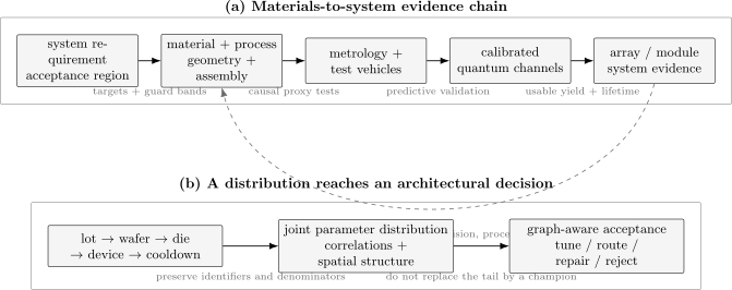
The materials–fabrication interface is a closed evidence chain. Requirements set an acceptance region; material, process, geometry, assembly, and environment variables produce a distribution of devices; metrology and test vehicles test causal hypotheses; calibrated quantum channels determine usable yield; and architecture-level evidence feeds back into design and process control. Tuning, routing, repair, and rejection are explicit outcomes, not missing denominators.
Let
collect material state , process history , geometry , assembly and package state , and operating environment . Let denote tunable controls and calibration parameters. The observed device vector can be written schematically as
where is the measurement protocol and includes measurement error and unresolved variation. The map is generally nonlinear, history-dependent, and many-to-many:
- one interface can contribute dielectric loss, charge noise, strain, and thermal resistance;
- one measured error can receive contributions from several materials and control channels;
- a process change can improve one metric while worsening another;
- calibration can hide static variation without removing noise or drift.
An architecture defines an acceptance event
Each indicator tests one required part of the architecture contract. The durable output of fabrication is therefore a distribution over , together with evidence that the measured distribution predicts membership in under the intended operating protocol.
Ten questions for a complete interface
Section titled “Ten questions for a complete interface”For each process and platform, record:
- Which microscopic or structural variables are believed to matter?
- Which of them are measured directly, and at what spatial scale?
- Which room-temperature or intermediate-temperature tests are used as proxies?
- What causal evidence connects each proxy to a cryogenic quantum metric?
- What is the joint distribution across lot, wafer, die, device, and cooldown?
- Which variation is static and calibratable, and which is noisy or drifting?
- Which acceptance rules were fixed before inspecting the best devices?
- What fractions were attempted, fabricated, electrically functional, calibrated, and usable?
- How do correlations and spatial clustering alter system yield?
- What changes after packaging, cooldown, aging, radiation exposure, or repeated service?
Quality, Uniformity, Yield, and Reliability
Section titled “Quality, Uniformity, Yield, and Reliability”These words answer different questions.
| Quantity | Question | Typical evidence |
|---|---|---|
| material identity | What phase, composition, isotope content, defect population, and interface were made? | diffraction, spectroscopy, microscopy, chemical analysis |
| material or component quality | How small is a loss, disorder, linewidth, or defect metric on a test structure? | resonator , mobility, optical linewidth, trap heating, gap hardness |
| targeting | Is the mean or median near the design value? | critical dimension, sheet resistance, junction resistance, resonance frequency |
| uniformity | How broad and spatially structured is the distribution? | wafer maps, matched pairs, within-die and between-lot variance |
| functional yield | What fraction passes structural or electrical tests? | continuity, leakage, threshold, coupling, source, detector, or trap tests |
| calibrated yield | What fraction can be initialized, controlled, measured, and kept within limits? | automated tune-up and held-out validation |
| system yield | Can a required connected set operate simultaneously under the architecture contract? | graph-aware acceptance and cycle-level tests |
| reliability | For how long and through how many cycles does the accepted state persist? | aging, thermal cycling, stress, drift, and survival data |
A high median with a heavy lower tail may be less useful than a modest but narrow distribution. A high component yield may coexist with low system yield if components fail in correlated regions or if their parameters cannot be jointly calibrated. A long-lived champion device says little about reliability unless the sampling rule, censoring, and service conditions are known.
From Physical Variation to Quantum Error
Section titled “From Physical Variation to Quantum Error”Static sensitivity and covariance
Section titled “Static sensitivity and covariance”Near a chosen operating point, a differentiable device model gives
If the linearization is adequate, covariance propagates as
The off-diagonal entries matter. A radial process gradient, common deposition step, shared source crystal, or package stress can move many components together. Reporting only one standard deviation per parameter discards the correlations that determine frequency collisions, shared-bias compatibility, decoder assumptions, and common-mode failure.
The Jacobian is local. It can fail near charge transitions, avoided crossings, mode hybridization, threshold voltages, percolation, crack formation, or a change of defect charge state. In those regimes, preserve the measured joint distribution or use a validated nonlinear model rather than forcing a Gaussian error bar through a discontinuity.
Noise transfer
Section titled “Noise transfer”For slowly varying parameters and an operating frequency , the leading frequency-noise spectrum is
Cross-spectra retain common fluctuators and correlated control noise. The equation also separates two interventions:
- reduce the noise source through material or process changes;
- reduce device susceptibility through geometry, encoding, bias choice, shielding, or control.
A sweet spot suppresses a first derivative. It does not prove that the underlying fluctuators disappeared, and second-order sensitivity, other quadratures, leakage, and drift can remain. One-Over-F Noise and Noise Spectra own the detailed conversion from spectra to protocol-dependent dephasing.
Participation turns material loss into device loss
Section titled “Participation turns material loss into device loss”Superconducting microwave devices provide a clear example of a transferable idea. If region stores a fraction of a mode’s electric energy and has an effective low-power loss tangent , a common model is
For a specified field convention,
This is not a universal microscopic theory. Loss tangents can depend on power, frequency, temperature, processing, field orientation, and the assumed thickness and permittivity of nanometer-scale interfaces. Several participation vectors are needed to identify several unknown losses. A single resonator cannot uniquely assign its loss to all interfaces.
The broader lesson is durable:
Material selection alone controls only part of that product.
Fabrication dispersion becomes control dispersion
Section titled “Fabrication dispersion becomes control dispersion”For a transmon with fixed charging energy,
Small junction-resistance variation then gives approximately
The sign is irrelevant to the relative standard deviation. This relation connects an accessible junction test to frequency targeting, but only under the stated fixed-, small-variation model. It does not predict coherence, coupler behavior, spectral collisions, or packaged-system yield by itself.
In a spin-qubit array, threshold, one-electron transition, valley-splitting, lever-arm, and tunnel-coupling distributions determine how many independent voltages and calibration steps are needed. In photonics, width and thickness variation change propagation constants and coupler ratios, which can be partly trimmed or thermally tuned at the cost of power and control channels. Static variation has become an architecture resource bill.
Material and Process Variables
Section titled “Material and Process Variables”Bulk host, composition, and isotope
Section titled “Bulk host, composition, and isotope”The host establishes band structure, phonons, nuclear spins, optical transitions, superconducting properties, thermal transport, and defect chemistry. Relevant records can include:
- source lot, growth method, orientation, thickness, stoichiometry, and intentional dopants;
- isotopic composition and its uncertainty;
- dislocation, vacancy, impurity, inclusion, and grain distributions;
- residual stress, strain gradients, domains, and texture;
- carrier density, mobility, resistivity, critical temperature, or optical absorption under a specified protocol.
Isotopic purification is a targeted intervention, not a synonym for general purity. Reducing spinful nuclei can suppress one magnetic bath while leaving charge traps, paramagnetic impurities, dislocations, interfaces, and control noise unchanged. Tyryshkin and collaborators’ seconds-scale donor-spin coherence in enriched silicon and Balasubramanian and collaborators’ isotope-engineered diamond experiments demonstrate the value of host isotope control under their respective protocols; they do not specify the yield or control quality of a fabricated processor.
Surfaces and interfaces
Section titled “Surfaces and interfaces”Quantum devices often concentrate fields and wavefunctions at boundaries: metal–substrate edges in a transmon, a semiconductor–oxide interface beneath a gate, the sidewall of a waveguide, the surface near a shallow color center, an ion above a trap electrode, or a semiconductor–superconductor interface in a hybrid device.
For every important interface, record:
- the two adjoining materials and any interlayer;
- formation order and whether the interface was made in situ;
- cleaning, air exposure, transfer, oxidation, annealing, and storage history;
- roughness, composition, thickness, strain, charge, and defect evidence;
- the relevant electric, magnetic, optical, mechanical, or thermal participation;
- stability under bias, illumination, cooldown, and time.
“Atomically sharp” in one microscopy cross-section is valuable structural evidence. It is not a wafer-level distribution, a low-noise measurement, or a quantum-channel benchmark. Conversely, improved coherence after an interface change is strong device evidence but may not identify which microscopic defect was removed unless the comparison controls geometry, processing, environment, and sampling.
Disorder, defects, and contamination
Section titled “Disorder, defects, and contamination”Defects can be desired qubits, useful dopants, benign spectators, fluctuators, loss centers, traps, scatterers, or leakage pathways. Their effect depends on identity, charge state, location, orientation, density, correlations, dynamics, and coupling to the mode.
A useful defect ledger distinguishes:
- designed defects, such as color centers or donors;
- intrinsic defects, such as vacancies, antisites, dangling bonds, and dislocations;
- process-induced defects, including implantation damage, plasma damage, redeposition, residues, and amorphized layers;
- environmental defects, including adsorbates, oxides, trapped charge, and radiation-induced excitations;
- effective fluctuators, inferred from spectra but not yet assigned a unique microscopic identity.
Do not turn an effective two-level fluctuator into a named chemical defect without direct evidence. A phenomenological model can be predictive while the microscopic assignment remains active research.
Geometry, registration, and dimensional control
Section titled “Geometry, registration, and dimensional control”Critical dimensions convert process variation into energy and coupling variation. Relevant quantities include line width, gap, overlap area, sidewall angle, etch depth, film thickness, junction area, waveguide cross-section, implant position, alignment, and layer-to-layer registration.
Use three values:
- designed: the layout or target;
- fabricated: the structure measured by calibrated metrology;
- effective: the parameter inferred from device behavior.
They need not agree. An effective electrical area can differ from a microscopy area because of barrier nonuniformity; an optical width can differ from a top view because sidewall angle matters; an implanted distribution is not a point at the nominal beam coordinate.
Stress, strain, and thermal mismatch
Section titled “Stress, strain, and thermal mismatch”Films, bonded dies, fibers, wire bonds, adhesives, lids, and cooldown contractions create mechanical boundary conditions. Strain can shift optical transitions, valley energies, tunnel couplings, magnetic anisotropy, resonator frequency, and defect stability. It can also crack, delaminate, or buckle a structure.
Measure strain where the active mode resides and after the relevant assembly and thermal cycle. A room-temperature wafer-curvature number may miss a local package-induced gradient at operating temperature. Strain can be a tunable resource, but the actuator range, hysteresis, noise, cross-coupling, and fatigue then belong in the control contract.
Assembly and package are part of the process
Section titled “Assembly and package are part of the process”Die attach, bonding, interposers, through-substrate vias, fiber attach, optical coupling, seams, magnetic materials, thermal anchors, and enclosure surfaces can change a previously screened die. Track pre-package and post-package metrics using stable identifiers. The package can add:
- electromagnetic and acoustic modes;
- dielectric, conductor, seam, and radiation loss;
- stress and thermal gradients;
- particle and chemical contamination;
- coupling variation and crosstalk;
- repair constraints and new common-cause failures.
An accepted bare die is not automatically an accepted module.
Cross-Platform Profiles
Section titled “Cross-Platform Profiles”The same evidence chain appears differently across platforms.
| Platform | High-leverage variables | Intermediate tests | Quantum and system consequences |
|---|---|---|---|
| superconducting circuits | substrate and metal loss, native oxides, junction barrier, residues, seams, critical dimensions | resonator loss, junction resistance, microscopy, wafer maps | , frequency targeting, flux or charge noise, collisions, package modes |
| silicon spins and donors | isotope fraction, heterostructure or oxide interface, gate stack, disorder, valley splitting, implant placement | threshold and one-electron voltages, mobility, charge sensing, tunnel maps | dephasing, initialization, exchange control, shared-bias compatibility, tune-up burden |
| defect and solid-state spins | host purity, isotope, defect creation, charge stability, strain, surface termination, nanophotonic processing | photoluminescence, linewidth, charge-state and site maps, cavity tests | spin coherence, optical indistinguishability, usable-emitter yield, spectral tuning |
| integrated photonics | film absorption, sidewall roughness, thickness, stress, coupler dimensions, detector stack, fiber attach | propagation loss, resonator , splitter ratios, detector and coupling maps | loss, phase error, source brightness, interference, heralding rate, thermal-tuning power |
| trapped ions | electrode surface, adsorbates, dielectrics, roughness, RF loss, optical integration | surface analysis, electrical test, resonator or trap test vehicles | motional heating, charging, trap depth, optical crosstalk, service life |
| neutral atoms | cell and coating materials, optics, wavefront quality, electrode and source surfaces | optical loss and wavefront maps, vacuum compatibility, lifetime tests | trap uniformity, scattering, Stark shifts, collision loss, array availability |
| hybrid and topological devices | epitaxy, intermixing, disorder, induced gap, electrostatics, contact and gate interfaces | structural analysis, normal transport, gap spectroscopy, charge stability | subgap states, poisoning, parity readout, tuning range, reproducibility |
| bosonic memories and converters | dielectric, piezoelectric, magnetic, optical, and acoustic loss; interfaces and mode overlap | multimode loss extraction, ringdown, spectroscopy, thermal response | memory lifetime, added noise, conversion efficiency, pump heating, mode crowding |
These entries are prompts, not platform verdicts. The relevant distribution depends on the architecture and protocol.
Superconducting circuits
Section titled “Superconducting circuits”Superconducting Qubits owns the complete circuit architecture. At the materials interface, three distinctions are especially important:
- a test resonator samples a different field distribution from a qubit;
- a junction-resistance distribution predicts only selected Hamiltonian parameters;
- a coherence improvement on isolated devices does not establish simultaneous yield in a connected processor.
Martinis and collaborators connected dielectric two-level systems to qubit loss. Wang and collaborators varied geometry to relate transmon relaxation to surface participation. Later tantalum, surface-encapsulation, and multimode loss studies showed how controlled material and geometry changes can improve or separate loss contributions. The durable method is comparative: hold the right variables fixed, vary participation or surface chemistry, measure enough independent devices, and test whether the inferred loss model predicts a new geometry.
Silicon spin devices
Section titled “Silicon spin devices”Silicon Spin Qubits owns encodings, exchange gates, shuttling, readout, and code evidence. The materials interface couples isotope and heterostructure quality to a dense gate stack. An industrial process can have excellent gate continuity while still requiring better one-electron voltage uniformity, valley splitting, tunnel control, and low-frequency charge noise.
The correct denominator changes by stage: gates, dots, complete dot arrays, devices reaching one-electron occupation, spin qubits, calibrated pairs, and simultaneously operable arrays. Shared-voltage or crossbar architectures impose a joint acceptance window that individually tunable research devices do not.
Defect spins and quantum emitters
Section titled “Defect spins and quantum emitters”Defect and Solid-State Spin Qubits owns host families, registers, optical interfaces, and network-node evidence. Fabrication must coordinate a desired defect’s number, position, orientation, isotope, charge state, spin bath, optical frequency, and coupling to a nanostructure. Improving placement can add damage; bringing a center near a surface can improve field sensitivity or optical coupling while worsening charge and spin noise.
Large-scale optical mapping is therefore part of manufacturing, not a cosmetic characterization step. Dory and collaborators demonstrated registration and automated spectroscopy across many fields of view, illustrating how stable identifiers and scalable screening connect emitter discovery to device integration. Screening is not deterministic creation, but it can convert a sparse distribution into a characterized and routable resource.
Integrated photonics
Section titled “Integrated photonics”Photonic Qubits owns source, encoding, interference, detection, feed-forward, and loss accounting. Waveguide loss accumulates with path length; splitter and phase errors compose through interferometers; fiber and chip coupling affect accepted throughput; and thermal trimming trades fabrication tolerance for power and calibration.
A process design kit for quantum photonics needs more than nominal geometry. It needs distributions for low-power loss, phase, couplers, sources, detectors, cryogenic shifts, and package interfaces under the photon statistics and wavelengths of use. Classical high-power optical tests can miss absorption, heating, fluorescence, detector behavior, or noise relevant at the single-photon level.
Trapped ions and neutral atoms
Section titled “Trapped ions and neutral atoms”The qubits are atoms, but fabricated surfaces still define their environment. For trapped ions, electrode adsorbates, dielectrics, processing, temperature, and distance affect electric-field noise and motional heating. Hite and collaborators’ in situ cleaning experiment reduced heating by two orders of magnitude in the tested trap, strong evidence that surface state can be causal. It did not establish one universal adsorbate mechanism for every material, temperature, or process.
For neutral atoms, fabricated optics, coatings, electrodes, cells, and source assemblies affect wavefronts, light shifts, vacuum compatibility, and service cycles. Trapped-Ion Qubits and Neutral-Atom and Rydberg Qubits own the platform contracts; the cross-platform lesson is that “atomic qubit” does not mean “materials-independent apparatus.”
Hybrid and topological devices
Section titled “Hybrid and topological devices”Topological Qubits separates materials, signatures, nonlocal encodings, parity operations, and logical architectures. Epitaxial semiconductor–superconductor interfaces produced much harder induced gaps than earlier soft-gap devices, demonstrating a decisive materials advance. A hard gap is still not proof of a topological phase, Majorana mode, protected qubit, or fault-tolerant operation.
For frontier devices, preserve the full evidence ladder:
Skipping an arrow converts a materials result into an architecture overclaim.
The Metrology Ladder
Section titled “The Metrology Ladder”No single instrument spans atomic structure, wafer uniformity, cryogenic transport, and quantum channels. A mature process uses a ladder in which each stage answers a different question.
Incoming-material qualification
Section titled “Incoming-material qualification”Incoming tests establish source identity and broad uniformity before expensive processing:
- composition, isotope, phase, orientation, thickness, and surface state;
- impurity, dislocation, defect, stress, and roughness distributions;
- electrical, optical, magnetic, mechanical, and thermal properties under a specified protocol;
- source lot, storage, shipping, handling, and shelf-age records.
Sampling must match the possible spatial structure. One central measurement cannot exclude an edge gradient, localized inclusion, growth sector, or lot-to-lot shift.
In-line process control
Section titled “In-line process control”In-line measurements test whether the process remained within its controlled state. Critical dimensions, film thickness, sheet resistance, junction or contact test structures, alignment marks, particles, wafer curvature, and surface chemistry may provide fast feedback. These measurements are valuable because they occur before packaging and low-temperature testing, but their connection to quantum performance must be demonstrated rather than presumed.
End-of-line functional tests
Section titled “End-of-line functional tests”Room-temperature or moderate-temperature tests can reject opens, shorts, leakage, gross threshold errors, dead detectors, broken heaters, failed optical paths, and out-of-range junctions. A functional test should state:
- the stimulus, environment, and instrument uncertainty;
- the pass region and guard band;
- false-pass and false-reject consequences;
- whether the tested structure is the active device or a nearby proxy;
- how the result changes after packaging and cooldown.
Cryogenic screening
Section titled “Cryogenic screening”Cryogenic probes can measure resonators, junctions, charge transitions, optical lines, detector response, trap impedances, and other properties before a die enters the most resource-intensive system. Screening temperature matters. A spin device characterized at may reveal electrostatic yield without proving millikelvin initialization or gate fidelity. A superconducting test resonator can rank films without sampling a junction, qubit capacitor, package seam, or processor radiation environment.
Quantum-channel validation
Section titled “Quantum-channel validation”The decisive layer measures accepted operations under the intended context: state preparation, gates, idle channels, leakage, measurement, reset, memory, links, or sensing response. Validation should include simultaneous operation, drift, representative power, and held-out data where those conditions define the architecture.
Metrics for Quantum Hardware owns metric definitions. Control, Readout, and Calibration owns estimators, validation, drift tracking, and feedback. Here the issue is whether those quantum metrics can be traced back to material and process variables with useful predictive power.
System and lifetime validation
Section titled “System and lifetime validation”The final layer asks whether accepted components remain usable as a connected system:
- required graph and frequency allocation;
- concurrent gates, readout, reset, or optical paths;
- package and thermal interactions;
- calibration time and control-resource limits;
- repeated cycles and logical or task-level behavior;
- uptime, aging, repair, and replacement.
Materials evidence has reached the architecture only when it predicts this layer or a clearly stated intermediate layer.
Test Vehicles and Proxy Validity
Section titled “Test Vehicles and Proxy Validity”A test vehicle deliberately emphasizes a material, interface, process, or failure mechanism while remaining cheaper or easier to measure than the full device. Examples include:
- resonators with varied surface participation;
- junction arrays with several areas and perimeter-to-area ratios;
- Hall bars, transistors, and charge sensors beside spin-qubit arrays;
- waveguides and rings with varied widths, bends, and claddings;
- witness coupons for microscopy and chemistry;
- trap surfaces compatible with both surface analysis and ion sensing;
- optical cavities or registration patterns around emitter material.
Good test vehicles form a designed matrix. If there are candidate loss regions with unknown strengths, use several geometries with sufficiently different participation vectors. In a linear loss model,
where , is the participation of region in vehicle , and is its effective loss tangent. If the columns of are nearly dependent, the inferred are not separately identifiable. More devices do not repair a poorly conditioned design matrix.
A proxy is useful when it is:
- physically connected to the target;
- measured with lower cost or earlier in the process;
- stable across the intended domain;
- predictive on held-out lots, wafers, or devices;
- accompanied by uncertainty and a decision rule.
Correlation on the development data is not enough. A process change can alter the relation between proxy and target. Revalidate after changes in material source, geometry, equipment, recipe, package, firmware, or operating temperature.
Screening is a classification problem
Section titled “Screening is a classification problem”Let be a screening pass and the event that a device is usable after full calibration. A useful report includes
Precision depends on the base rate . A screen validated only on hand-selected good and bad examples can appear excellent while performing poorly on production prevalence. False rejects waste devices; false passes waste scarce packaging, cryogenic, and calibration capacity. The threshold should be chosen from those costs and the architecture, not from classification accuracy alone.
Yield Is a Joint Probability
Section titled “Yield Is a Joint Probability”For device observables and acceptance region , define
The region is multivariate. A device may pass coherence, frequency, leakage, and readout limits separately yet fail their joint requirement or a simultaneous-operation test.
The all-good estimate is usually only a warning
Section titled “The all-good estimate is usually only a warning”If components are independent, identically distributed, all required, and each has usable probability , then
At , an all-good 1,000-component assembly has probability . The lesson is not that every architecture needs perfect component yield. It is that a large system needs some combination of higher yield, redundant capacity, repair, reconfiguration, modularity, replacement, or acceptance of partial connectivity.
Real devices violate the simple model:
- a shared process step creates correlated failures;
- spatial clustering makes nearby components fail together;
- calibration and routing can rescue some nominal variation;
- a code or compiler may tolerate disabled components only in certain patterns;
- modules can be preselected and connected after test;
- one common package defect can disable many otherwise good devices.
A graph-aware system yield is better written by separating two events. Let mean that contains the required subgraph, and let mean that . Then
The required subgraph may encode code distance, routing, detector coverage, optical connectivity, control conflicts, and spare capacity. Yield simulation should sample measured spatial and cross-parameter correlations rather than randomly permuting components until those correlations disappear.
Keep the denominators separate
Section titled “Keep the denominators separate”Report a flow such as
State why units left the flow. Excluding known failures from a coherence histogram may be appropriate for a conditional physics question, but it cannot support an unconditional process-yield claim.
Hierarchical Variation and Uncertainty
Section titled “Hierarchical Variation and Uncertainty”Measurements are nested. A simple random-effects model for an observable is
where , , , , and label lot, wafer, die, device, and cooldown. The terms represent variation at each level. Repeated shots or spectra belong below this hierarchy and estimate measurement or temporal variation; they do not create new wafers or devices.
This decomposition supports different interventions:
- lot variation points toward source material or major process shifts;
- wafer gradients point toward growth, deposition, thermal, or tool nonuniformity;
- die or local variation points toward patterning, defects, or neighborhood;
- device variation points toward critical dimensions or local fluctuators;
- cooldown variation points toward packaging, trapped charge, contamination, thermal history, or calibration.
Treat random-effects labels as statistical structure, not microscopic proof. The model can localize a scale without identifying a mechanism.
A yield estimate needs an interval
Section titled “A yield estimate needs an interval”If of exchangeable units pass and a uniform beta prior is used, the posterior for an unknown pass probability is
Its mean is , and credible intervals remain wide when is small. The prior and exchangeability assumptions must be stated. A distribution-free frequentist interval is also acceptable. Reporting “100% yield” after five devices without an interval is not.
The experimental unit follows the intervention. If a recipe was applied once to one wafer containing 1,000 structures, that study has rich within-wafer information but only one independent wafer-level intervention. Do not use the structure count as the replication count for the process change.
Process capability is conditional
Section titled “Process capability is conditional”For a stable, approximately normal scalar process with lower and upper specification limits LSL and USL, one common capability index is
combines centering and spread. It is not a universal quantum-hardware score. It can mislead for skewed, multimodal, drifting, censored, or spatially correlated data, and a capable proxy process is useful only if its specification predicts the quantum acceptance region. Show the distribution and control state, not just the index.
Design for Manufacturability and Calibratability
Section titled “Design for Manufacturability and Calibratability”Fabrication and architecture can trade resources. A robust design is not necessarily the one with the best nominal performance; it is the one whose performance remains acceptable over the measured process distribution and operating history.
Allocate a variation budget
Section titled “Allocate a variation budget”For target , the linearized variance is
Use this budget to identify dominant combinations, then decide whether to:
- tighten a material or process distribution;
- redesign geometry to reduce sensitivity;
- move the operating point;
- add trim or tuning range;
- improve metrology and feed-forward;
- add redundancy or routing flexibility;
- relax a specification that does not affect the system objective.
Do not allocate every variable independently when covariance terms dominate.
Tuning is not free
Section titled “Tuning is not free”Tuning can rescue static offsets, but it consumes:
- control channels, digital memory, DAC range, and resolution;
- calibration time and recurring drift checks;
- thermal power and wiring;
- spectral space and crosstalk margin;
- algorithm or compiler constraints;
- reliability margin in actuators and feedback.
A wide tuning range can also introduce loss or noise. Report as-fabricated spread, post-tuning spread, resources consumed, and residual drift separately.
Guard bands depend on measurement uncertainty
Section titled “Guard bands depend on measurement uncertainty”An acceptance limit at the architecture boundary is not automatically the same as a manufacturing test limit. If measurement uncertainty, aging, packaging shift, or model error can move a passing part outside the system region, use a guard band justified by a decision-risk analysis. The Guide to the Expression of Uncertainty in Measurement supplies the general measurement framework; the system model supplies the consequence of a wrong decision.
Architecture can absorb known defects
Section titled “Architecture can absorb known defects”Options include spare components, tunable couplers, frequency allocation, defect-aware mapping, photonic switching, redundant emitters, replaceable modules, post-fabrication trim, and logical codes adapted to erasure or bias. These mechanisms require measured defect maps, stable identifiers, and validated error behavior. “The compiler will route around it” is not an architecture until routing overhead, connectivity, calibration, and failure correlations have been evaluated.
Reliability, Aging, and Change Control
Section titled “Reliability, Aging, and Change Control”Yield is measured at an acceptance time. Reliability concerns survival after acceptance. For a time-dependent hazard ,
A constant hazard gives , but quantum hardware often has history-dependent failure:
- oxide growth, adsorption, diffusion, corrosion, and charge trapping;
- junction-resistance or optical-coupling drift during storage;
- thermal-cycle stress, delamination, bond failure, and package relaxation;
- laser, microwave, voltage, pump, or radiation damage;
- cryopump saturation and contamination;
- actuator fatigue and repeated retuning;
- software or calibration changes that expose a latent hardware limit.
Distinguish calendar age, powered hours, cold hours, thermal cycles, optical or microwave dose, and operation cycles. Right-censored units that have not yet failed contain information and should not be discarded.
Preserve a configuration identity
Section titled “Preserve a configuration identity”A quantum result should be traceable to:
- source materials and lots;
- process traveler and recipe versions;
- mask and design revision;
- tools, maintenance state, and deviations;
- metrology and test-vehicle data;
- die, device, and package identifiers;
- cooldown and infrastructure configuration;
- firmware, calibration, and analysis versions;
- repair, rework, storage, and aging history.
After a process change, decide what must be requalified. A new surface clean may alter both loss and junction contact; a new dielectric can change capacitance, charge noise, stress, and thermal behavior; a package revision can invalidate bare-die screening correlations.
Learning Causally from Process Changes
Section titled “Learning Causally from Process Changes”A process correlation becomes useful engineering knowledge only when alternative explanations are constrained.
Design comparisons around the causal question
Section titled “Design comparisons around the causal question”Prefer:
- split lots or matched wafers processed together;
- randomized assignment of treatments to wafer positions or devices;
- blocking by lot, wafer, die region, tool, and measurement session;
- common geometry and package when testing a material change;
- several geometries when testing a participation model;
- blinded or automated analysis where discretionary selection is possible;
- predeclared primary metrics, exclusions, and acceptance thresholds;
- replication at the level where the treatment was applied;
- a held-out confirmation batch after optimization.
One-factor-at-a-time experiments can be interpretable but inefficient and can miss interactions. Factorial or response-surface designs are useful when several controllable variables plausibly interact, provided the physical constraints and independent-unit count are respected.
Negative and positive controls
Section titled “Negative and positive controls”A negative control tests whether the measurement or handling process creates the apparent effect. A positive control verifies sensitivity to a known change. Witness structures can separate a film property from the complete device, and multiple participation geometries can distinguish an interface change from a global environmental shift.
Failure analysis closes the loop
Section titled “Failure analysis closes the loop”Preserve rejected and failed units long enough to ask:
- Is the failure spatially clustered?
- Which upstream metrology changed?
- Did the device fail structurally, electrically, during cooldown, during calibration, or under simultaneous operation?
- Can destructive analysis identify a mechanism?
- Does the proposed mechanism predict an independent observable?
- Does the corrective action improve the next held-out batch?
Failure categories should be allowed to evolve, but changes in the taxonomy must be versioned so historical yield remains interpretable.
Dated Evidence and Its Limits
Section titled “Dated Evidence and Its Limits”The following examples illustrate the interface as of August 2026. They are not a ranking of platforms.
- Superconducting foundry processing, 2024. Van Damme and collaborators reported an industry-standard 300-mm process with measurements of 400 transmon qubits and 12,840 junction test structures. They reported a across-wafer qubit yield, time-averaged and echo coherence exceeding , spatial frequency variation, and aging data. This established a substantial manufacturability result. It did not establish the yield of a fully connected error-corrected processor.
- Spin-qubit wafer screening, 2024. Neyens and collaborators tested 232 twelve-dot devices on a representative 300-mm wafer. They reported more than 10,000 working gates, quantum-dot yield, and full-device yield under their electrical definitions. Yet their common-voltage analysis estimated a median of of dots per device could reach one-electron occupation together. High component yield and shared-control compatibility were visibly different metrics.
- Automated emitter metrology, 2023. Dory and collaborators registered color centers to machine-readable coordinates, parallelized resonant spectroscopy with a reported two-orders-of-magnitude speedup, and automated chip-scale imaging. The work advanced scalable screening and longitudinal identity; it did not imply deterministic creation of identical emitters.
- Integrated photonic manufacturing, 2025. A 300-mm silicon-photonics platform integrated sources, circuits, detectors, and packaging and reported high conditional component benchmarks. The publication explicitly separated fidelity conditioned on detection from loss. System resource accounting must preserve that distinction.
- Surface intervention in ion traps, 2012. In situ argon-ion cleaning reduced the measured heating rate by a factor of about 100 in the tested system while surface analysis tracked contamination. This was strong causal evidence for a surface contribution, not a complete universal microscopic model of anomalous heating.
- Materials and geometry co-design, 2024. Ganjam and collaborators used a multimode participation analysis, tantalum, annealed sapphire, and geometry optimization to realize on-chip microwave memories with measured – energy-relaxation times and – single-photon Ramsey times. The result illustrates predictive co-design; transferring it to another geometry requires a new participation and process validation.
- Hybrid-interface quality, 2015 onward. Epitaxial semiconductor–superconductor structures produced hard induced gaps and reduced one major ambiguity of earlier soft-gap devices. Gap hardness is a component property. The stronger sequence from nonlocal observables to encoded parity operations and protection scaling remains separately tested.
Evidence ladder
Section titled “Evidence ladder”Use the strongest label actually supported:
- material evidence: composition, structure, defect, or intrinsic-property measurement;
- test-vehicle evidence: a process-dependent loss, noise, or transport metric;
- single-device evidence: a calibrated qubit, mode, emitter, detector, or trap;
- distribution evidence: independent devices across relevant batches and locations;
- integrated-component evidence: sources, control, readout, and package operate together;
- array evidence: simultaneous calibrated operation with mapped failures and correlations;
- logical or task evidence: the material and process support the claimed encoded cycle, network service, sensing protocol, or workload;
- manufacturing evidence: controlled process, predictive screening, change control, yield, reliability, and repeatable output over time.
Reaching one rung does not make lower-rung work unimportant. It limits the noun used in the claim.
Reporting Contract
Section titled “Reporting Contract”A compact materials-to-system report is
At minimum, publish or preserve:
- intended architecture and acceptance region;
- material, process, geometry, assembly, and environment identifiers;
- sampling plan and all relevant denominators;
- maps and joint distributions, not only means and champions;
- uncertainty, censoring, exclusions, and missing-data rules;
- proxy definitions and held-out predictive performance;
- pre- and post-package, pre- and post-tuning metrics;
- calibration resources and simultaneous-operation context;
- failure taxonomy, repair, and disabled-component policy;
- aging interval, thermal cycles, stress exposure, and last review date;
- analysis code, model version, and enough provenance to reproduce the decision.
Proprietary details can limit disclosure, but omitted process or selection information must also limit the strength and reproducibility of the claim.
Common Mistakes
Section titled “Common Mistakes”- Naming a material instead of specifying its state. Lot, phase, composition, isotope, surface, interface, and process history matter.
- Treating a champion as a process. Show independent-device and batch distributions.
- Calling electrical continuity qubit yield. Preserve functional, calibrated, simultaneous, and system-level denominators.
- Assuming proxy validity. Test prediction on held-out devices and after process changes.
- Ignoring covariance. Correlated shifts determine shared control, collisions, and common-cause failure.
- Counting structures as process replicates. Replication follows the level of treatment.
- Attributing every effective fluctuator to one defect chemistry. Separate predictive phenomenology from microscopic identification.
- Assuming tuning erases fabrication variation. Report tuning resources, noise, drift, and residual spread.
- Using room-temperature performance as a quantum metric. State exactly what the screen establishes.
- Equating a hard induced gap with a topological qubit. Preserve the evidence ladder.
- Ignoring packaging and cooldown. Compare stable identifiers before and after integration.
- Reporting yield without uncertainty. Include intervals and sampling assumptions.
- Hiding rejected units. Selection is part of the process outcome.
- Changing recipes without requalifying the proxy model. Version the complete chain.
A Practical Workflow
Section titled “A Practical Workflow”- Name the system objective. Start with a cycle, task, link, or sensing requirement.
- Define the acceptance region. Include joint metrics, graph constraints, drift, power, latency, and reliability.
- Build the causal ledger. Map material, process, geometry, assembly, and environment variables to device observables.
- Allocate sensitivity and variation budgets. Include covariance and nonlinear thresholds.
- Design test vehicles and controls. Make candidate mechanisms identifiable.
- Preserve hierarchy and provenance. Track lots through cooldown and calibration.
- Validate proxies prospectively. Use held-out batches and explicit screening costs.
- Estimate graph-aware yield and reliability. Include tuning, repair, reconfiguration, and common-cause failures.
- Close the loop. Feed failures and system data into the next controlled design or process revision.
Exercises
Section titled “Exercises”1. Participation-limited lifetime
Section titled “1. Participation-limited lifetime”A mode has two dielectric contributions:
Neglect other loss. Estimate . Then halve without changing the frequency or loss tangents. By what factor does improve?
Solution
The total inverse quality factor is
Using with ,
After halving ,
so
The improvement is , not exactly two, because the second loss channel remains.
2. Correlated fabrication shifts
Section titled “2. Correlated fabrication shifts”Two resonances have fluctuations and , each with standard deviation and correlation coefficient . Find the standard deviation of their detuning . Compare with independent fluctuations.
Solution
For equal standard deviations ,
With and ,
For independent shifts, and . A common process shift can broaden absolute frequencies while partly canceling in a local detuning. The same correlation could be harmful for a different architecture metric.
3. Scaling an all-required assembly
Section titled “3. Scaling an all-required assembly”An architecture needs all components and assumes independent usable probability per component.
- Estimate the all-good yield.
- Explain why a measured component yield is still insufficient to predict a real processor yield.
Solution
The simple estimate is
The approximation uses . The real system may have spatially correlated failures, several component types, parameter-window failures, package defects, repair, spares, routing around faults, and graph constraints. The component number and the architecture’s acceptance rule are both needed.
4. Clustered failures
Section titled “4. Clustered failures”One hundred devices are arranged in ten process blocks of ten. In a simplified model, each complete block is good with probability and bad otherwise, independently between blocks. Every device therefore has marginal good probability .
- Find the probability that all 100 devices are good.
- Compare with 100 independent devices of yield .
- What does the comparison teach?
Solution
All devices are good only when all ten blocks are good:
Under independent device failures,
Positive within-block correlation increases the probability of a completely good assembly here, but failures occur in ten-device clusters. An architecture that tolerates a few isolated failures may fare much worse under the clustered model. Marginal component yield does not determine system yield; the failure geometry and acceptance rule do.
5. Uncertainty behind a yield claim
Section titled “5. Uncertainty behind a yield claim”Nineteen of twenty independently sampled devices pass a fixed test. Using a uniform prior for pass probability :
- write the posterior distribution;
- find its mean;
- explain why neither nor the posterior mean should be advertised without an interval and sampling context.
Solution
The posterior is
Its mean is
The raw fraction is , but twenty observations leave substantial uncertainty about the underlying probability. The inference also assumes exchangeable independent units sampled from the intended process. Twenty devices from one selected die do not establish lot-level yield.
6. Process capability
Section titled “6. Process capability”A stable scalar process has mean , standard deviation , lower specification limit , and upper specification limit . Compute and identify the limiting side.
Solution
The two one-sided values are
Thus , limited by the upper specification. The calculation does not show that the process is stable, normal, uncorrelated, or predictive of a quantum metric; those assumptions require separate evidence.
7. Screening precision
Section titled “7. Screening precision”A cryogenic screen has sensitivity and specificity for final device usability. Only of incoming devices are actually usable. Find the probability that a screened-pass device is usable.
Solution
Let and be the usable and unusable contributions. Bayes’ rule gives
Despite apparently respectable sensitivity and specificity, only about of passing devices are usable because the base rate is low. Screening thresholds must be evaluated on production prevalence and decision costs.
8. Identifiability in a loss experiment
Section titled “8. Identifiability in a loss experiment”Two test resonators have participation vectors
for two unknown interface losses. Can their measurements determine both loss tangents? Propose a useful third participation vector.
Solution
No. The second vector is exactly one half of the first, so the participation matrix has rank one. Both measurements constrain the same weighted sum .
A useful third design must not be proportional, for example
The expanded matrix has rank two. In practice, uncertainty and near collinearity still matter, so one should inspect its conditioning and use more than the minimum number of independently fabricated vehicles.
9. Design a split-lot experiment
Section titled “9. Design a split-lot experiment”A team believes a new surface clean lowers superconducting-device loss. Design a comparison that can distinguish the clean from wafer location, geometry, package, cooldown, and measurement-session effects.
Solution
Use at least several independent wafers or lots. Within each, randomize matched dies or resonator geometries between the old and new clean, while blocking by wafer region. Keep downstream geometry and package fixed, or balance package variants across both treatments. Measure witness surfaces and several participation geometries, then interleave device measurements within the same sessions and cryogenic environment.
Predeclare the primary loss metric, exclusions, and hierarchy-aware analysis. After model development, repeat the comparison on a held-out batch and test whether inferred loss factors predict a geometry not used in the fit. The independent replication count is the number of independently treated process units, not the number of repeated spectra.
10. Audit a frontier claim
Section titled “10. Audit a frontier claim”A report states: “An epitaxial interface produced a hard induced gap, proving that the process yields protected topological qubits.” Separate what follows from what does not.
Solution
A hard induced gap supports the claim that the measured hybrid interface strongly suppressed subgap conductance under the reported spectroscopy conditions. With structural controls and replication, it can establish a reproducible materials and component advance.
It does not by itself prove a topological phase, non-Abelian excitation, nonlocal encoding, parity-measurement fidelity, quasiparticle-poisoning lifetime, universal gate set, protection scaling, or manufacturing yield. Those claims require additional observables and distributions at successive rungs of the evidence ladder.
Summary
Section titled “Summary”Materials and fabrication matter through a chain, not a label. Source materials, interfaces, dimensions, defects, assembly, and environment create a joint distribution of device parameters. Geometry and state susceptibility convert that distribution into loss, noise, dispersion, and drift. Metrology and test vehicles can provide early proxies only when their causal and predictive links survive held-out validation. Calibration can rescue static variation, but it consumes control, power, time, and stability margin.
Trustworthy scaling claims therefore report hierarchy, covariance, acceptance regions, denominators, graph-aware yield, aging, and failures. A mature process is not merely capable of making an exceptional component. It repeatedly makes traceable components that become usable channels and remain usable in the intended architecture.
References
Section titled “References”- Y. Y. Gao, M. A. Rol, S. Touzard, and C. Wang, “A practical guide for building superconducting quantum devices,” PRX Quantum 2, 040202 (2021), doi:10.1103/PRXQuantum.2.040202.
- J. M. Martinis et al., “Decoherence in Josephson qubits from dielectric loss,” Physical Review Letters 95, 210503 (2005), doi:10.1103/PhysRevLett.95.210503.
- C. Wang et al., “Surface participation and dielectric loss in superconducting qubits,” Applied Physics Letters 107, 162601 (2015), doi:10.1063/1.4934486.
- A. P. M. Place et al., “New material platform for superconducting transmon qubits with coherence times exceeding milliseconds,” Nature Communications 12, 1779 (2021), doi:10.1038/s41467-021-22030-5.
- M. Bal et al., “Systematic improvements in transmon qubit coherence enabled by niobium surface encapsulation,” npj Quantum Information 10, 43 (2024), doi:10.1038/s41534-024-00840-x.
- A. P. Read et al., “Precision measurement of the microwave dielectric loss of sapphire in the quantum regime with parts-per-billion sensitivity,” Physical Review Applied 19, 034064 (2023), doi:10.1103/PhysRevApplied.19.034064.
- S. Ganjam et al., “Surpassing millisecond coherence in on chip superconducting quantum memories by optimizing materials and circuit design,” Nature Communications 15, 3687 (2024), doi:10.1038/s41467-024-47857-6.
- J. Van Damme et al., “Advanced CMOS manufacturing of superconducting qubits on 300 mm wafers,” Nature 634, 74–79 (2024), doi:10.1038/s41586-024-07941-9.
- A. M. Tyryshkin et al., “Electron spin coherence exceeding seconds in high-purity silicon,” Nature Materials 11, 143–147 (2012), doi:10.1038/nmat3182.
- J. Yoneda et al., “A quantum-dot spin qubit with coherence limited by charge noise and fidelity higher than ,” Nature Nanotechnology 13, 102–106 (2018), doi:10.1038/s41565-017-0014-x.
- A. M. J. Zwerver et al., “Qubits made by advanced semiconductor manufacturing,” Nature Electronics 5, 184–190 (2022), doi:10.1038/s41928-022-00727-9.
- S. Neyens et al., “Probing single electrons across 300-mm spin qubit wafers,” Nature 629, 80–85 (2024), doi:10.1038/s41586-024-07275-6.
- G. Balasubramanian et al., “Ultralong spin coherence time in isotopically engineered diamond,” Nature Materials 8, 383–387 (2009), doi:10.1038/nmat2420.
- M. Sutula et al., “Large-scale optical characterization of solid-state quantum emitters,” Nature Materials 22, 1338–1344 (2023), doi:10.1038/s41563-023-01644-8.
- A. Sipahigil et al., “An integrated diamond nanophotonics platform for quantum-optical networks,” Science 354, 847–850 (2016), doi:10.1126/science.aah6875.
- R. A. Parker et al., “A diamond nanophotonic interface with an optically accessible deterministic electronuclear spin register,” Nature Photonics 18, 156–161 (2024), doi:10.1038/s41566-023-01332-8.
- M. W. Puckett et al., “422 million intrinsic quality factor planar integrated all-waveguide resonator with sub-MHz linewidth,” Nature Communications 12, 934 (2021), doi:10.1038/s41467-021-21205-4.
- PsiQuantum Team, “A manufacturable platform for photonic quantum computing,” Nature 641, 876–883 (2025), doi:10.1038/s41586-025-08820-7.
- D. A. Hite et al., “100-fold reduction of electric-field noise in an ion trap cleaned with in situ argon-ion-beam bombardment,” Physical Review Letters 109, 103001 (2012), doi:10.1103/PhysRevLett.109.103001.
- K. R. Brown et al., “Materials challenges for trapped-ion quantum computers,” Nature Reviews Materials 6, 892–905 (2021), doi:10.1038/s41578-021-00292-1.
- K. S. McKay et al., “Measurement of electric-field noise from interchangeable samples with a trapped-ion sensor,” Physical Review A 104, 052610 (2021), doi:10.1103/PhysRevA.104.052610.
- P. C. Holz et al., “Electric-field noise in a high-temperature superconducting surface ion trap,” Physical Review B 104, 064513 (2021), doi:10.1103/PhysRevB.104.064513.
- P. Krogstrup et al., “Epitaxy of semiconductor–superconductor nanowires,” Nature Materials 14, 400–406 (2015), doi:10.1038/nmat4176.
- W. Chang et al., “Hard gap in epitaxial semiconductor–superconductor nanowires,” Nature Nanotechnology 10, 232–236 (2015), doi:10.1038/nnano.2014.306.
- Ö. Gül et al., “Ballistic superconductivity in semiconductor nanowires,” Nature Communications 8, 16025 (2017), doi:10.1038/ncomms16025.
- M. Reagor et al., “Quantum memory with millisecond coherence in circuit QED,” Physical Review B 94, 014506 (2016), doi:10.1103/PhysRevB.94.014506.
- K. K. Mehta et al., “Integrated optical multi-ion quantum logic,” Nature 586, 533–537 (2020), doi:10.1038/s41586-020-2823-6.
- R. J. Niffenegger et al., “Integrated multi-wavelength control of an ion qubit,” Nature 586, 538–542 (2020), doi:10.1038/s41586-020-2811-x.
- Joint Committee for Guides in Metrology, Evaluation of Measurement Data—Guide to the Expression of Uncertainty in Measurement, JCGM 100:2008 (2008), doi:10.59161/JCGM100-2008E.
- NIST/SEMATECH, e-Handbook of Statistical Methods (National Institute of Standards and Technology), doi:10.18434/M32189.
- D. C. Montgomery, Design and Analysis of Experiments, 10th ed. (Wiley, 2019).
- D. K. Schroder, Semiconductor Material and Device Characterization, 3rd ed. (Wiley, 2006), doi:10.1002/0471749095.
Further Connections
Section titled “Further Connections”- Device Fabrication Concepts owns process flows, contacts, gates, assembly, encapsulation, provenance, acceptance tests, and batch reproducibility.
- Nanostructures for Quantum Technology develops the wider relation among confinement, fabrication, control, calibration, and architecture.
- Quantum Materials by Design develops the discovery loop from target properties through synthesis, characterization, and validation.
- Disorder in Quantum Matter owns disorder ensembles, correlation functions, lifetimes, localization, and phase consequences.
- Hardware Overview supplies the platform-neutral encoding–control–readout–infrastructure contract.
- Metrics for Quantum Hardware defines coherence, channel, leakage, crosstalk, throughput, logical, and workload metrics.
- Control, Readout, and Calibration develops estimators, validation, calibration dependencies, drift monitoring, and feedback.
- Cryogenic and Vacuum Infrastructure owns the post-fabrication thermal, wiring, shielding, gas-load, diagnostic, recovery, and availability boundary.
- Modular Architectures carries module yield, qualification, interchangeability, repair, and failure correlation into topology, scheduling, and system availability.
- Superconducting Qubits, Silicon Spin Qubits, and Defect and Solid-State Spin Qubits provide detailed solid-state architecture cases.
- Photonic Qubits, Trapped-Ion Qubits, and Topological Qubits show how fabrication evidence enters optical, atomic, and frontier hybrid systems.