Device Fabrication Concepts
A quantum-material device is not a pristine Hamiltonian with wires attached afterward. Patterning changes boundaries; contacts exchange charge and broaden states; gates create electric fields and trap dynamics; dielectrics screen interactions; transfer creates strain and interfaces; etching creates edges and defects; packaging sets thermal, electromagnetic, and mechanical boundary conditions. Fabrication is therefore part of the physical preparation of the system.
This page is the canonical home for process flow, contacts, gates, assembly, encapsulation, process provenance, acceptance tests, device denominators, and batch reproducibility. Materials and Fabrication Interface owns the technology-facing translation from those material and process distributions to quantum channels, calibration burden, usable-system yield, reliability, and architecture evidence.
This page is intentionally not a cleanroom recipe. Process temperatures, chemicals, vacuum conditions, dose windows, etch gases, safety controls, and compatible material stacks are facility- and material-specific. The durable principles are instead:
- translate the intended observable into device requirements;
- identify every interface and process step that can change the active degrees of freedom;
- preserve a process record tied to structural and electrical metrology;
- characterize the packaged device again after cooldown;
- report distributions and failures, not only the best surviving device.
A useful evidence ladder is:
- process intent: mask geometry, layer sequence, contact and gate design, materials, and acceptance criteria;
- fabricated structure: measured dimensions, composition, interfaces, defects, alignment, and continuity;
- functional device: contacts conduct, gates tune, leakage is bounded, and the intended terminals are electrically isolated;
- calibrated low-temperature system: carrier density, contact transparency, electron temperature, filtering, cross-capacitance, and drift are measured in the operating environment;
- reproducible physics result: the target observable survives device, batch, cooldown, and analysis controls.
An optical micrograph proves geometry at optical resolution. It does not prove a clean interface, an ohmic contact, a known carrier density, or a cold electronic distribution.
Canonical Scope
Section titled “Canonical Scope”This page is the canonical home for cross-platform fabrication concepts and process provenance in quantum-matter devices. It owns the route from a material and measurement requirement to contacts, gates, patterning, assembly, encapsulation, process-induced disorder, cryogenic packaging, acceptance tests, yield reporting, and batch-level reproducibility.
van der Waals Heterostructures owns atomically thin stack physics, alignment, gate architecture, interlayer tunneling, and interface evidence. Engineered Heterostructures owns cross-platform proximity transfer and interface self-energies. Transport Measurements owns terminal configurations, four-terminal reduction, reversal, sweep protocols, and electrical uncertainty budgets.
Disorder in Quantum Matter owns disorder ensembles, correlations, lifetimes, and disorder-controlled phases. Nanostructures for Quantum Technology owns the system-level relation among fabrication yield, calibration, control, and architecture. Quantum Materials by Design owns the wider discovery loop from target property through synthesis and validation. Here the organizing question is narrower: what physical system did fabrication actually create, and how is that fact preserved through measurement?
The Fabricated Hamiltonian
Section titled “The Fabricated Hamiltonian”Begin with a device ledger
Section titled “Begin with a device ledger”A schematic low-energy decomposition is
The terms need not be separately measurable or even sharply separable. The equation is a ledger: it prevents a nominally passive fabrication element from disappearing from the model. A metal contact can contribute electrostatic doping, hybridization, strain, screening, spin–orbit coupling, exchange, superconducting pairing, and dissipation at once.
A device cross-section should identify:
- active material, thickness, composition, crystal axes, and relevant surfaces or edges;
- substrate, buffer, encapsulant, spacer, dielectric, and adhesion layers;
- contact material, geometry, overlap, interface preparation, and lead routing;
- local and global gates, dielectric thicknesses, and grounded conductors;
- patterned dimensions and the metrology method defining them;
- expected current paths, voltage probes, leakage paths, and capacitive couplings;
- thermal anchors, filters, radiation shields, and mechanical constraints.
Use “nominal” for a mask or deposition target and “measured” for a post-process dimension. Sidewall angle, overetch, undercut, redeposition, line-edge roughness, film stress, and grain structure can make the two differ.
A process flow is a sequence of interventions
Section titled “A process flow is a sequence of interventions”A generic process can include material growth or exfoliation, identification, transfer or epitaxy, lithography, etching, cleaning, deposition, lift-off, annealing, dicing, wire bonding, and packaging. Each intervention has an intended transformation and possible collateral transformations. A process traveler should therefore record, for every step:
- incoming sample state and identifier;
- equipment, recipe version, date, operator, and material lot;
- actual measured parameters, not only setpoints;
- deviations, rework, queue time, and air or solvent exposure;
- outgoing metrology and acceptance decision.
The traveler is scientific data. Without it, correlations between a low-temperature anomaly and a process excursion cannot be reconstructed.
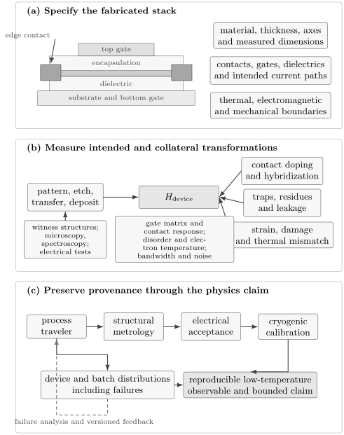
A fabricated device combines the intended stack with contact, electrostatic, strain, disorder, and environmental terms. Structural metrology, room-temperature acceptance, and cryogenic calibration connect the process traveler to a physics claim; failures feed back into the process model rather than being silently discarded.
Contacts
Section titled “Contacts”A contact is a reservoir and an interface
Section titled “A contact is a reservoir and an interface”An electrical contact should be specified by what it must do. It may need to inject equilibrium carriers, sense voltage with negligible current, define a tunnel barrier, preserve spin or valley polarization, induce superconductivity, transmit microwaves, or remain noninvasive to a fragile state. “Low resistance” is not sufficient for all of these tasks.
At a metal–semiconductor interface, work-function mismatch, interface dipoles, surface states, chemical bonding, and electrostatic screening determine band bending and carrier injection. The elementary Schottky–Mott picture is often modified by Fermi-level pinning. At a metal–two-dimensional-material interface, top contacts, edge contacts, residues, damage, and metal-induced doping produce distinct boundary conditions. At a normal–superconductor interface, transparency and disorder determine whether the contact acts as an ordinary reservoir, tunnel probe, or proximity source.
Useful contact observables include:
- two- and four-terminal resistance versus temperature, gate, bias, and field;
- contact linearity and symmetry in current–voltage curves;
- transfer-length or multiple-length structures;
- stability under thermal cycles and current stress;
- noise, drift, telegraph switching, and electromigration;
- spectroscopic evidence for a tunnel barrier or induced gap;
- spatial evidence for contact doping, reaction, or delamination.
An apparently linear – curve over one bias window does not prove an ohmic microscopic interface. Thermal broadening, parallel conduction, or an overly narrow window can hide a barrier.
Transfer-length bookkeeping
Section titled “Transfer-length bookkeeping”For a uniform sheet of width contacted by two approximately identical contacts, a simple length series gives
The intercept estimates twice the lumped contact resistance and the slope estimates the sheet resistance under the model’s assumptions. Nonuniform doping near contacts, current crowding, width variation, invasive voltage probes, and ballistic transport can invalidate the linear interpretation.
For a distributed contact with specific contact resistivity and sheet resistance , define the transfer length
In the standard transmission-line approximation,
where is the contact length. For , extending the contact farther gives little benefit because most current transfers within a few of the edge. This model is a diagnostic, not a universal law for coherent, edge-state, tunneling, superconducting, or strongly inhomogeneous contacts.
Contacts can be invasive
Section titled “Contacts can be invasive”A voltage probe is noninvasive only when the current it draws and the equilibration it causes are negligible for the intended observable. In a coherent conductor, a contact can absorb phase information and redistribute populations. In a two-dimensional channel, the metal can screen gates and alter density beneath the overlap. In a small island, the contact capacitance and tunnel rate become terms in the Hamiltonian.
A contact ledger should state:
- interface type and intended transport regime;
- materials, thicknesses, deposition order, and any adhesion layer;
- contact area or edge length and its measured uncertainty;
- interface exposure, cleaning, damage, and vacuum break;
- contact resistance or transparency in the relevant state;
- induced doping, strain, exchange, pairing, or screening;
- maximum safe current density and evidence for stability.
Conductance Quantization owns the channel-transmission and contact-resistance limits of coherent transport. Proximity and Andreev Physics owns superconducting-interface scattering and induced states.
Gates and Electrostatics
Section titled “Gates and Electrostatics”Geometric capacitance is the first approximation
Section titled “Geometric capacitance is the first approximation”For a parallel-plate dielectric of thickness and relative permittivity , the geometric capacitance per area is
If is a signed carrier density, positive for electron accumulation under the chosen convention, an ideal isolated gate gives
absorbs built-in potentials and fixed charge. This conversion fails when quantum capacitance, trap charging, fringing fields, multiple conductors, depletion, dielectric nonlinearity, or mobile ions matter.
The quantum capacitance per area is
For a simple series geometry,
Near a low density of states, can be the smaller capacitance, so a substantial fraction of gate voltage changes chemical potential rather than electrostatic field across the dielectric. Interface traps add frequency- and history-dependent charge; representing them by one series capacitor is generally inadequate.
Multiple gates require a capacitance matrix
Section titled “Multiple gates require a capacitance matrix”For conductors indexed by ,
The matrix includes intended gates, contacts, reservoirs, screening planes, and parasitic couplings. Local gates often affect several device parameters at once. A virtual-gate transformation can diagonalize a measured response locally, but it drifts when traps switch or the operating point changes.
For a simple dual-gated two-dimensional layer, one common convention is
here is an electric-displacement coordinate with units of charge per area; some literature divides it by or reverses its sign. State the convention. The offset voltages and should be calibrated from charge-neutrality, quantum Hall, compressibility, or another measured feature rather than assumed from zero instrument voltage.
Gate quality is multidimensional
Section titled “Gate quality is multidimensional”A gate stack should be tested for:
- leakage current and its temperature, field, polarity, and sweep-rate dependence;
- dielectric breakdown and soft pre-breakdown damage;
- hysteresis, relaxation, and charge jumps;
- cross-capacitance to contacts and neighboring gates;
- spatial nonuniformity and fringe-field confinement;
- dielectric loss and microwave heating;
- displacement-current artifacts during sweeps;
- stability across cooldowns and illumination history.
The average electric field is only a screening estimate. Local fields concentrate at edges, particulates, pinholes, thickness steps, and sharp metal corners. A device operated once near nominal breakdown may be permanently changed even if it does not short.
Heterostructure Assembly
Section titled “Heterostructure Assembly”Nominal sequence is not local structure
Section titled “Nominal sequence is not local structure”Layered devices can be grown directly, wafer-bonded, transferred, picked up, stamped, laminated, or assembled through combinations of these methods. The durable requirements are to know:
- layer identity, thickness, polytype, and orientation before assembly;
- sequence, overlap area, intended registry, and exposed interfaces;
- temperature, atmosphere, pressure, and residence time relevant to adhesion or reaction;
- local twist, strain, bubbles, wrinkles, tears, folds, and trapped contamination afterward;
- whether later lithography, etching, or annealing changed the buried interface.
In rotationally sensitive systems, the fabrication angle is a target, not the final local twist field. Elastic relaxation and heterostrain can create domains and spatially varying moiré periods. Structural and spectroscopic metrology should therefore be linked to the actual transport or optical region.
van der Waals Heterostructures develops the stack Hamiltonian, alignment diagnostics, gate architecture, and interface evidence. Moiré Superlattices owns the relation between measured local geometry and miniband scales. The fabrication page records how those inputs were realized and where the process can bias them.
Selection begins before measurement
Section titled “Selection begins before measurement”Fabrication yield is conditional on upstream choices. Researchers may select the largest flake, the cleanest-looking region, the stack with the fewest visible bubbles, and the device with working contacts. That can be sensible, but the denominator must be preserved:
only if the stage yields are meaningfully defined and their conditional probabilities are multiplied in the correct order. The factors are usually correlated. A thick flake may survive transfer but fail electrostatic control; a process that improves contact yield may increase channel disorder.
Report the number of candidate materials inspected, stacks attempted, devices patterned, devices electrically continuous, devices cooled, and devices included in the scientific analysis. A final histogram without this flow can hide strong survivorship bias.
Encapsulation
Section titled “Encapsulation”Encapsulation can isolate an active material from oxygen, water, polymers, adsorbates, ion motion, mechanical abrasion, and direct lithographic exposure. It can also provide an atomically flatter dielectric environment and enable edge contacts. For air-sensitive materials, the atmosphere and time between exfoliation, assembly, and sealing can determine whether the intended phase survives at all.
Encapsulation is not physically neutral. It changes:
- dielectric screening and therefore Coulomb interactions and exciton binding;
- electrostatic disorder and gate capacitance;
- strain, thermal contraction, pressure, and wrinkle formation;
- heat flow and optical interference;
- surface phonons and remote scattering;
- chemical potential through trapped charge or residues;
- access for scanning probes, adsorbates, or local gates.
An encapsulation ledger should identify material, thickness, source lot, crystallographic alignment when relevant, exposed edges, sealing completeness, atmosphere, transfer polymer, post-assembly treatment, and aging tests. “Encapsulated” does not imply “clean,” and a high mobility does not establish an atomically residue-free interface.
Cleanliness and Process-Induced Disorder
Section titled “Cleanliness and Process-Induced Disorder”Clean means fit for an observable
Section titled “Clean means fit for an observable”No single cleanliness metric covers every experiment. A surface can be sufficiently free of charged disorder for high mobility yet unsuitable for scanning tunneling because of sparse adsorbates. A tunnel junction can be electrically uniform while containing enough magnetic defects to broaden a spin-sensitive spectrum. A contact can be low resistance but chemically react with the active layer.
Common process-induced perturbations include:
| Source | Possible device term | Useful control |
|---|---|---|
| polymer or solvent residue | doping, traps, tunnel barrier, adsorbate scattering | witness surface, AFM, spectroscopy, alternate resist or protected interface |
| plasma or ion damage | vacancies, edge disorder, amorphization, implanted charge | dose split, Raman or microscopy, protected control region |
| etch redeposition | leakage path, edge doping, contact barrier | cross-section, sidewall inspection, electrical isolation test |
| metal diffusion or reaction | alloyed contact, gap states, magnetic or superconducting proximity | composition depth profile, temperature-budget split |
| trapped interface contamination | bubbles, local strain, dielectric gaps | optical, AFM, Raman, local transport or scanning probe |
| dielectric charge traps | hysteresis, drift, telegraph noise, density puddles | sweep-rate, time, temperature, frequency, illumination tests |
| film stress and thermal mismatch | strain, cracks, delamination, symmetry change | wafer curvature, Raman, diffraction, cooldown cycling |
| particulate or pinhole | local field concentration, gate leakage, shorts | dark-field inspection, leakage maps, breakdown statistics |
Cleaning and annealing are interventions, not erasers. They may remove one residue while mobilizing another contaminant, reacting a contact, changing stoichiometry, relaxing twist, creating vacancies, or increasing diffusion. Every cleaning step needs a before-and-after observable and a compatible control.
Mobility is not a purity certificate
Section titled “Mobility is not a purity certificate”In a simple band,
The transport lifetime weights momentum relaxation. Quantum oscillation or spectroscopic linewidths can instead constrain a single-particle lifetime , which weights scattering differently. Smooth disorder can give a large ratio, while rare strong defects may dominate local behavior without greatly changing average mobility.
Characterize disorder at the scale relevant to the claim:
- composition and crystallinity for bulk or epitaxial defects;
- surface and interface topography for roughness and bubbles;
- Raman, optical, or diffraction maps for strain and domains;
- density inhomogeneity and compressibility for electrostatic puddles;
- low-frequency noise for active traps;
- transport and quantum lifetimes for angular scattering;
- device-to-device distributions for process variability.
Disorder in Quantum Matter owns the statistical classification and physical consequences of these perturbations.
Cryogenic Measurement Environment
Section titled “Cryogenic Measurement Environment”The electron temperature must be demonstrated
Section titled “The electron temperature must be demonstrated”The refrigerator’s thermometer measures a location in the cryostat, not necessarily the electronic distribution in the device. Joule power in a resistive element is
for a lumped linear element. In a common low-temperature phenomenology, electron–phonon cooling is
so a steady state gives
, volume , and exponent depend on material, dimensionality, disorder, and temperature range. The expression is a diagnostic model, not a universal thermometer. Contact cooling, photon exchange, substrate phonons, and nonequilibrium distributions may dominate.
Demonstrate electronic temperature with a calibrated noise, Coulomb-blockade, quantum-dot, superconducting, or other primary or secondary thermometer near the active device when low-energy claims depend on it. Excitation-amplitude extrapolation and dwell-time tests help separate saturation from intrinsic behavior.
Wiring defines bandwidth and noise
Section titled “Wiring defines bandwidth and noise”A simple line resistance and shunt capacitance have
At frequencies , a resistor’s one-sided open-circuit Johnson voltage-noise density is
Real cryogenic lines contain distributed capacitance and inductance, thermoelectric junctions, dielectric loss, resonances, ground loops, amplifier backaction, triboelectric noise, and radio-frequency leakage. Filtering trades bandwidth and settling time against noise and heating. A nominal lock-in frequency can still mix with line resonances or gate displacement currents.
A cryogenic integration record should include:
- wire material, gauge, routing, shielding, and thermal anchors at each stage;
- room-temperature and cryogenic filters, attenuation, cutoff, and measured transfer function;
- source and detector impedances, compliance, input bias, and grounding;
- sample mount, connector, bond-wire, and contact configuration;
- thermometer location, thermalization evidence, and excitation-power sweep;
- magnetic materials, trapped-flux procedure, vector alignment, and field-dependent heating;
- illumination, radiation shielding, vacuum, pressure medium, and thermal-cycle history.
Thermal contraction can strain a thin crystal or break a marginal contact. Magnetic field can heat metallic parts through eddy currents during a sweep. Gate lines can carry radio-frequency noise directly to a small electron system. Packaging is therefore the final fabrication step.
Reproducibility
Section titled “Reproducibility”Preserve the hierarchy
Section titled “Preserve the hierarchy”Measurements are nested: repeated sweeps belong to one cooldown; cooldowns belong to one device; devices belong to one chip, flake, wafer region, or stack; those belong to a fabrication batch and source material. Repeated sweeps do not substitute for independent devices.
A simple variance-components model is
where is a batch effect, is a device-within-batch effect, and is repeat-level variation. Even when a formal mixed-effects fit is not justified, this hierarchy should determine plots and error summaries.
Report:
- number of batches, source crystals or wafers, devices, cooldowns, and repeats;
- prespecified inclusion, exclusion, and acceptance rules;
- distributions of dimensions, contact resistance, leakage, mobility, density offset, and target observables;
- failed devices and their failure stage;
- recipe changes and which data used each version;
- representative devices chosen by a declared rule, not visual preference;
- raw and processed data linked to design and process identifiers.
Yield needs uncertainty
Section titled “Yield needs uncertainty”If of devices pass a prespecified test, the observed yield is
The denominator and test matter as much as the percentage. “Working” might mean room-temperature continuity, gate tunability, target base-temperature behavior, or survival through cycling. State which.
If all devices pass and independent Bernoulli trials are a reasonable first model, a one-sided exact lower confidence bound at confidence is
Twenty successes out of twenty do not establish a process: at one-sided confidence, the lower bound is about . Batch correlations make the effective information smaller still.
Architecture-level all-good yield and calibration scaling belong to Nanostructures for Quantum Technology. The present concern is process evidence: whether a reported device is typical of a documented fabrication population.
Change one thing and keep a witness
Section titled “Change one thing and keep a witness”A strong process comparison uses:
- contemporaneous control and modified devices from comparable starting material;
- randomized or interleaved processing when tool drift matters;
- witness substrates or structures that isolate deposition, etch, contact, or dielectric properties;
- blinded analysis or prespecified metrics where selection is consequential;
- enough batches to distinguish a recipe effect from a good source crystal or a favorable tool day.
Optimization on the same devices used to claim improvement gives an optimistic estimate. Hold-out devices or later batches provide a more honest test.
A Fabrication-to-Claim Workflow
Section titled “A Fabrication-to-Claim Workflow”Before fabrication
Section titled “Before fabrication”- Define the observable, operating range, and required terminal geometry.
- Convert those requirements into contact, gate, interface, thermal, and bandwidth specifications.
- Identify material incompatibilities and cumulative temperature, chemical, radiation, and air-exposure budgets.
- Define structural, room-temperature, and cryogenic acceptance tests.
- Assign identifiers linking source material, design file, mask, recipe, and intended measurement.
During fabrication
Section titled “During fabrication”- Record actual process values and deviations in a versioned traveler.
- Measure critical dimensions and interfaces at informative checkpoints.
- Preserve witness structures and dose, thickness, or treatment splits.
- Stop or quarantine samples when an acceptance criterion fails; do not silently relabel rework.
- Record the denominator at every selection step.
Before a physics claim
Section titled “Before a physics claim”- Verify continuity, isolation, leakage, contact response, gate range, and electrostatic stability.
- Recalibrate after cooldown and after major field, thermal, or illumination history.
- Bound electron temperature, excitation heating, line bandwidth, and environmental drift.
- Compare devices and batches using the correct nested hierarchy.
- Test whether the claimed feature correlates with contact, geometry, disorder, or process variables.
- Preserve failures and null devices as evidence about alternatives.
| Claim | Required fabrication evidence |
|---|---|
| intrinsic material transport | geometry, noninvasive contacts, density calibration, disorder and heating controls |
| gate-induced phase | leakage, displacement current, hysteresis, density or field calibration, sweep history |
| proximity-induced state | parent integrity, interface coupling, spatial confinement, electrostatic and heating alternatives |
| twist-controlled behavior | local angle, strain, domains, active-region registration, device-to-device comparison |
| edge-dominated response | measured edge geometry, bulk leakage bounds, contact equilibration, length and nonlocal tests |
| reproducible platform | batch and device distributions, yield definition, failure ledger, cooldown stability |
Common Mistakes
Section titled “Common Mistakes”- Treating the mask as the device. Measure critical dimensions, layer overlap, and active-region registration after processing.
- Calling every linear contact ohmic. Test bias, temperature, gate, polarity, and current-density dependence.
- Using four terminals as proof that contacts are irrelevant. Voltage probes can be invasive and contacts can dope or equilibrate the channel.
- Converting gate voltage to density with geometry alone. Quantum capacitance, traps, screening, and multiple gates may matter.
- Using nominal twist angle as a local material parameter. Relaxation, strain, and domains require local metrology.
- Equating encapsulation with cleanliness. Buried residues, bubbles, charge, and strain can remain.
- Calling mobility a complete disorder metric. It emphasizes transport scattering and can miss local or quantum broadening.
- Assuming an anneal only cleans. It can diffuse, react, desorb, create vacancies, or relax the structure.
- Equating refrigerator and electron temperature. Heating, noise, and weak thermal coupling require an electronic check.
- Reporting only successful devices. Preserve attempted, rejected, failed, cooled, and analyzed denominators.
- Treating many sweeps on one device as replication. Device and batch variability require higher-level repeats.
- Changing a recipe without versioning it. A process improvement is not reproducible if data cannot be assigned to a precise process state.
Exercises
Section titled “Exercises”Exercise 1: Extract contact and sheet resistance
Section titled “Exercise 1: Extract contact and sheet resistance”A family of equal-width devices obeys a linear fit
The width is . Find the contact resistance per contact and sheet resistance. In the long-contact approximation, estimate and .
Solution
The intercept is , so
The slope is . Therefore
For ,
Since
we obtain
Finally,
The numerical extraction is meaningful only if current spreading, contact-induced density, geometry, and transport regime satisfy the transmission-line model.
Exercise 2: Geometric and quantum capacitance
Section titled “Exercise 2: Geometric and quantum capacitance”A two-dimensional channel is separated from a gate by of dielectric with . Estimate the induced carrier density for using geometric capacitance. What happens if ?
Solution
The geometric capacitance per area is
The ideal signed density magnitude is
If , the series capacitance is
The induced density at the same voltage is therefore half the geometric estimate. This ideal series result still neglects traps, contacts, and fringe fields.
Exercise 3: Construct independent dual-gate coordinates
Section titled “Exercise 3: Construct independent dual-gate coordinates”A device has . Find a voltage change that changes displacement coordinate while keeping signed density fixed.
Solution
Fixed density requires
With ,
The corresponding displacement-coordinate change is
Thus follows a constant-density line while tuning . Measured capacitances and offset drift should replace nominal values in a real device.
Exercise 4: Estimate electron overheating
Section titled “Exercise 4: Estimate electron overheating”A metallic device follows an electron–phonon model with and . The phonon temperature is and the dissipated power is . Estimate .
Solution
Use
The two terms are
and
Therefore
Only raises the model electron temperature to about . The result demonstrates why base-temperature claims need excitation sweeps and electronic thermometry. It is not transferable to a different material without checking its cooling law.
Exercise 5: Audit a gate-sweep anomaly
Section titled “Exercise 5: Audit a gate-sweep anomaly”A resistance peak appears only when a top gate is swept upward faster than . It shifts on the downward sweep and becomes larger after illumination. List the leading fabrication or environment alternatives to an equilibrium gate-induced phase transition and design controls.
Solution
Leading alternatives include dielectric or interface traps, mobile ions, leakage-induced heating, displacement-current pickup, slow contact doping, photoactivated charge, and an instrument settling artifact. The history and illumination dependence already show that gate voltage alone is not a complete state variable.
Useful controls are:
- record gate current and dissipated power simultaneously;
- vary sweep rate over decades and include stepped sweeps with long dwell times;
- compare up, down, and closed-loop histories;
- measure after fixed waiting times at selected voltages;
- repeat in darkness after controlled illumination and thermal reset;
- monitor a nearby charge sensor or capacitance channel;
- test whether the feature follows density calibrated by Hall or quantum oscillations;
- compare devices with different dielectric thicknesses, gate areas, and trap-processing controls.
An equilibrium phase boundary should converge as rate and waiting-time effects are removed. Persistent history dependence may still be interesting physics, but it requires a nonequilibrium claim.
Exercise 6: Put uncertainty on perfect observed yield
Section titled “Exercise 6: Put uncertainty on perfect observed yield”All devices in one fabrication batch pass a prespecified room-temperature continuity test. Find the one-sided exact lower confidence bound on the independent-device pass probability.
Solution
For successes out of ,
with . Thus
The result supports “observed yield , with a one-sided lower bound of about under independent Bernoulli sampling.” It does not support a known process. One batch also leaves batch-to-batch variation unconstrained.
Exercise 7: Design a reproducibility test
Section titled “Exercise 7: Design a reproducibility test”A laboratory reports a correlated state in the single device with the highest mobility among twelve devices made from three source crystals. The state appears after a new anneal. Design a test that separates anneal effect, source-material effect, and selection bias.
Solution
Use several source crystals and divide comparable devices from each source between the old and new anneals. Interleave the processing order so tool drift and calendar time are not confounded with recipe. Prespecify structural, electrical, and scientific acceptance metrics before examining the target state. Preserve all attempted devices and report failures.
Analyze the hierarchy by source crystal, anneal, fabrication batch, device, and cooldown. Compare full distributions rather than only each group’s best device. Include witness samples that measure contact, residue, and stoichiometry changes caused by the anneal. Repeat the target measurement after independent cooldowns, and hold out a later batch that was not used to tune the anneal.
This design can reveal whether the new anneal shifts the population, whether one source crystal dominates both mobility and the state, and whether selecting the maximum created the apparent association. Twelve repeatedly measured devices still provide only twelve device-level units, not the number of sweeps collected.
Research Status
Section titled “Research Status”- Established: lithographic, deposition, etch, transfer, contact, gate, encapsulation, packaging, and cryogenic-integration principles; capacitance and transmission-line benchmarks; process metrology; nested replication and uncertainty reporting.
- Platform dependent: contact chemistry, Fermi-level pinning, dielectric traps, cleaning efficacy, annealing windows, encapsulation benefits, transfer yield, electron–phonon cooling, and the relation between room-temperature acceptance and low-temperature performance.
- Active: wafer-scale low-disorder two-dimensional integration, deterministic twist and strain control, residue-free patterning, damage-free contacts, in situ interface metrology, automated cryogenic calibration, and causal process optimization with limited device counts.
- Unsupported when omitted: an intrinsic or reproducible device claim that lacks process identifiers, contact and gate controls, electron-temperature evidence, device denominators, or independent device and batch replication.
Connections
Section titled “Connections”- How Quantum Matter Is Measured supplies the general record-to-observable-to-claim contract.
- Data Interpretation and Pitfalls audits how process variation, contact invasiveness, selected devices, and cooldown history constrain the eventual physics claim.
- Transport Measurements owns terminal configurations, reversal, geometry conversion, sweep control, contact loading, and electrical uncertainty.
- Hall Measurements supplies carrier-density, field-parity, and gate-calibration checks.
- Scanning Tunneling Microscopy and Spectroscopy explains why surface preparation and local cleanliness differ from transport cleanliness.
- van der Waals Heterostructures owns stack assembly, alignment, gate architecture, tunneling, and interface physics.
- Two-Dimensional Materials owns platform-wide electrostatics, dielectric screening, environmental sensitivity, and dimensionality evidence.
- Engineered Heterostructures develops proximity transfer and interface claim ladders.
- Superconducting Proximity Effect turns measured layer thicknesses, interface resistance, elastic scales, and parent degradation into a spatial pairing and inverse-proximity calculation; this page retains process provenance, interface metrology, and device-yield evidence.
- Moiré Superlattices develops local twist, strain, domain, and filling-scale calibration.
- Disorder in Quantum Matter classifies process-induced random potentials, roughness, defects, and active fluctuators.
- One-Over-f Noise develops trap ensembles, drift, telegraph noise, and low-frequency spectra.
- Conductance Quantization owns coherent channel, reservoir, and contact-resistance physics.
- Nanostructures for Quantum Technology connects fabrication distributions and calibration to system-level operation.
- Materials and Fabrication Interface carries process distributions into technology-specific quantum channels, predictive screening, graph-aware yield, calibration cost, reliability, and architecture claims.
- Quantum Materials by Design places device survival and reproducibility at the end of the materials-discovery loop.
References
Section titled “References”- S. M. Sze and K. K. Ng, Physics of Semiconductor Devices, 3rd ed. (Wiley, 2006), doi:10.1002/0470068329.
- D. K. Schroder, Semiconductor Material and Device Characterization, 3rd ed. (Wiley, 2006), doi:10.1002/0471749095.
- J. Bardeen, “Surface States and Rectification at a Metal Semi-Conductor Contact,” Physical Review 71, 717–727 (1947), doi:10.1103/PhysRev.71.717.
- A. Allain, J. Kang, K. Banerjee, and A. Kis, “Electrical Contacts to Two-Dimensional Semiconductors,” Nature Materials 14, 1195–1205 (2015), doi:10.1038/nmat4452.
- L. Wang et al., “One-Dimensional Electrical Contact to a Two-Dimensional Material,” Science 342, 614–617 (2013), doi:10.1126/science.1244358.
- C. R. Dean et al., “Boron Nitride Substrates for High-Quality Graphene Electronics,” Nature Nanotechnology 5, 722–726 (2010), doi:10.1038/nnano.2010.172.
- A. K. Geim and I. V. Grigorieva, “Van der Waals Heterostructures,” Nature 499, 419–425 (2013), doi:10.1038/nature12385.
- F. Pizzocchero et al., “The Hot Pick-Up Technique for Batch Assembly of van der Waals Heterostructures,” Nature Communications 7, 11894 (2016), doi:10.1038/ncomms11894.
- A. V. Kretinin et al., “Electronic Properties of Graphene Encapsulated with Different Two-Dimensional Atomic Crystals,” Nano Letters 14, 3270–3276 (2014), doi:10.1021/nl5006542.
- P. J. Zomer, M. H. D. Guimarães, J. C. Brant, N. Tombros, and B. J. van Wees, “Fast Pick Up Technique for High Quality Heterostructures of Bilayer Graphene and Hexagonal Boron Nitride,” Applied Physics Letters 105, 013101 (2014), doi:10.1063/1.4886096.
- R. Frisenda et al., “Recent Progress in the Assembly of Nanodevices and van der Waals Heterostructures by Deterministic Placement of 2D Materials,” Chemical Society Reviews 47, 53–68 (2018), doi:10.1039/C7CS00588C.
- M. Ishigami, J. H. Chen, W. G. Cullen, M. S. Fuhrer, and E. D. Williams, “Atomic Structure of Graphene on SiO,” Nano Letters 7, 1643–1648 (2007), doi:10.1021/nl070613a.
- A. Pirkle et al., “The Effect of Chemical Residues on the Physical and Electrical Properties of Chemical Vapor Deposited Graphene Transferred to SiO,” Applied Physics Letters 99, 122108 (2011), doi:10.1063/1.3643444.
- F. C. Wellstood, C. Urbina, and J. Clarke, “Hot-Electron Effects in Metals,” Physical Review B 49, 5942–5955 (1994), doi:10.1103/PhysRevB.49.5942.
- J. P. Pekola et al., “Limitations in Cooling Electrons Using Normal-Metal–Superconductor Tunnel Junctions,” Physical Review Letters 92, 056804 (2004), doi:10.1103/PhysRevLett.92.056804.
- D. V. Averin and K. K. Likharev, “Coulomb Blockade of Single-Electron Tunneling, and Coherent Oscillations in Small Tunnel Junctions,” Journal of Low Temperature Physics 62, 345–373 (1986), doi:10.1007/BF00683469.
- F. Pobell, Matter and Methods at Low Temperatures, 3rd ed. (Springer, 2007), doi:10.1007/978-3-540-46360-3.
- D. C. Montgomery, Design and Analysis of Experiments, 10th ed. (Wiley, 2019). Develops randomization, blocking, factorial design, and variance-aware process comparison.
- Joint Committee for Guides in Metrology, Evaluation of Measurement Data—Guide to the Expression of Uncertainty in Measurement, JCGM 100:2008 (2008), doi:10.59161/JCGM100-2008E.
- NIST/SEMATECH, e-Handbook of Statistical Methods (National Institute of Standards and Technology), doi:10.18434/M32189.
Summary
Section titled “Summary”Fabrication converts a material into a particular open, gated, contacted, strained, disordered, and thermally anchored quantum system. Trustworthy device physics begins with a measured cross-section and process traveler, continues through contact, gate, interface, leakage, disorder, and electron-temperature calibration, and ends with device- and batch-level distributions tied to prespecified acceptance rules. Contacts and encapsulants are not passive labels, geometric capacitance is not always carrier density, refrigerator temperature is not automatically electron temperature, and repeated sweeps are not independent devices. The process is mature when failures are informative, recipe changes are traceable, and the target result survives the full fabrication-to-cooldown hierarchy.