Engineered Heterostructures
An engineered heterostructure is a composite quantum system whose interface is designed to transfer, combine, or reshape selected properties of its constituents. A semiconductor may acquire pairing from a superconductor; a topological surface may acquire an exchange gap from a magnet; two insulating oxides may produce a conducting interface; or a cavity mode may hybridize with a material excitation. The useful object is not simply material A placed beside material B. It is the coupled system A–interface–B, including strain, electrostatics, disorder, electromagnetic boundary conditions, and contacts.
Three levels of claim must be kept separate:
- Constituent compatibility: both parent materials retain the properties needed for the design.
- Interfacial transfer: a response in one subsystem is demonstrably caused by coupling to the other.
- Engineered phase: the coupled device has a collective state, gap, invariant, or excitation structure that neither isolated constituent possesses.
The first two levels are established in many platforms. The third is established for some effects, such as ordinary superconducting proximity and exciton–polariton formation, but remains active or controversial for several proposed topological and cavity-stabilized phases.
Canonical Scope
Section titled “Canonical Scope”This page is the canonical home for cross-platform heterostructure design and evidence. It compares semiconductor–superconductor devices, magnetic–topological interfaces, polar oxide interfaces, and cavity–material hybrids, then gives a common claim ladder for proximity-engineered phases.
van der Waals Heterostructures owns atomically thin stack assembly, alignment, gating, vertical tunnelling, and the general interface self-energy construction. Superconducting Proximity Effect owns bulk real-space anomalous propagation, inverse suppression, and controlled clean or diffusive reductions. Proximity and Andreev Physics owns normal–superconductor scattering, BTK diagnostics, few-mode Andreev levels, and the detailed Majorana-device evidence baseline. Topological Insulators and Topological Superconductors own bulk invariants and boundary-mode derivations. Cavity QED owns the open quantum dynamics of discrete emitters and resonators.
Here the organizing question is different: what is the interface supposed to transfer, what else does it inevitably transfer, and which independent measurements establish the resulting state?
The Interface Design Ledger
Section titled “The Interface Design Ledger”A transferred property is a frequency-dependent response
Section titled “A transferred property is a frequency-dependent response”For two coupled sectors, the projected Green function of sector A can be written
The last line is the interface self-energy. Its Hermitian part shifts levels, changes velocities, opens avoided crossings, and can induce pairing or exchange. Its anti-Hermitian part describes escape and broadening when sector B has available states. Its frequency dependence redistributes spectral weight and renormalizes the parameters of A.
This compact expression explains why “stronger coupling” is not an unconditional improvement. Increasing can enlarge the desired induced scale while also:
- transferring disorder, quasiparticle poisoning, or dissipation;
- reducing the quasiparticle weight that remains in the controllable subsystem;
- producing charge transfer and band bending that move the chemical potential;
- straining or chemically reconstructing the interface;
- degrading the parent order through inverse proximity.
The full derivation and the distinction between hybridization, electrostatics, and proximity are developed in van der Waals Heterostructures.
Five quantities should be reported
Section titled “Five quantities should be reported”| Design quantity | Question | Representative measurements |
|---|---|---|
| parent integrity | do A and B retain their intended phases after fabrication? | diffraction, microscopy, magnetometry, parent-gap spectroscopy |
| interface structure | what termination, registry, strain, roughness, and chemistry are present? | STEM, EELS, X-ray probes, atom-resolved spectroscopy |
| coupling scale | how large and uniform is the transferred interaction? | anticrossings, induced gaps, exchange splitting, mode splitting |
| parasitic channels | what else crosses the interface? | subgap states, leakage, vacancies, heating, band bending |
| functional response | does the coupled system exhibit the target nonlocal or collective behavior? | transport, thermodynamics, spatial imaging, reciprocal control |
No single number replaces this ledger. An induced gap without its subgap density of states, an exchange splitting without the Fermi level, or a Rabi splitting without linewidths leaves the design problem underdetermined.
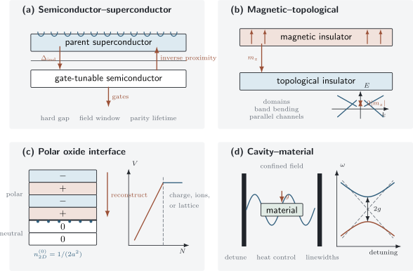
Four interface designs and their indispensable controls. Pairing, exchange, charge reconstruction, and photon hybridization are useful only when parent integrity, parasitic transfer, and a phase-specific measurement are tracked at the same time.
Semiconductor–Superconductor Devices
Section titled “Semiconductor–Superconductor Devices”The useful compromise
Section titled “The useful compromise”A low-density semiconductor provides electrostatic control, strong spin–orbit coupling, and a large effective factor; a conventional superconductor provides a condensate and a hard excitation gap. Epitaxial InAs–Al and related hybrids showed that atomic-scale interface control can greatly suppress the soft subgap continuum that limited earlier devices. Planar two-dimensional electron gases, selective-area networks, nanowires, and Josephson junctions now realize complementary geometries.
The design objective is not to maximize the induced gap alone. In a simple low-energy proximity model, stronger semiconductor–superconductor coupling increases the induced pairing toward the parent gap while moving spectral weight into the metal. The same process can reduce the semiconductor’s effective Zeeman and spin–orbit scales. A thin parent film can raise the critical field for a favorable orientation, yet orbital depairing, vortices, and disorder still constrain the usable field window.
A device therefore needs a simultaneous map of:
- the induced gap and residual subgap spectral weight;
- interface transparency and mode count;
- the semiconductor chemical potential and electrostatic profile;
- spin–orbit and effective Zeeman tensors after hybridization;
- parent critical field, shell thickness, and orbital response;
- quasiparticle poisoning, charge noise, and spatial nonuniformity.
The ordinary induced-gap self-energy and Andreev diagnostics are derived in Proximity and Andreev Physics.
Topological operation is a stricter claim
Section titled “Topological operation is a stricter claim”In the ideal uniform single-subband Rashba-wire model, the bulk transition is located by
with the topological side at larger while a reopened excitation gap survives. This equation is a model locator, not an experimental certification rule. Multiband occupation, smooth confinement, disorder, orbital coupling, parent-gap collapse, and interactions can all produce low-energy states outside its assumptions.
A local zero-bias peak is therefore insufficient. Stronger evidence includes a resolved bulk gap closing and reopening, correlated end response, length dependence, nonlocal conductance, calibrated temperature and lead transmission, parity-sensitive measurements, and eventually fusion or braid-order protocols. The retraction of a prominent quantized-conductance claim is a useful methodological reminder: full parameter ranges, raw calibration, and independent replication belong to the physics, not merely to data management.
Status: induced superconductivity, hard gaps, and gate-tunable Andreev spectra are established. Majorana-compatible signatures and increasingly sophisticated parity-control experiments are active research. As of August 2026, no semiconductor–superconductor platform has a universally accepted demonstration of topologically protected non-Abelian braiding.
Magnetic–Topological Interfaces
Section titled “Magnetic–Topological Interfaces”Which component of exchange opens the gap?
Section titled “Which component of exchange opens the gap?”The low-energy surface of an ideal three-dimensional topological insulator can be modeled as
An out-of-plane exchange component anticommutes with the kinetic term and opens a Dirac mass gap . Uniform in-plane components mainly shift the Dirac point in momentum in this minimal model. Real interfaces also add warping, potential disorder, hybridization, band bending, and symmetry-lowering terms, so magnetization by itself does not determine the spectrum.
The design must satisfy four conditions at once:
- the magnetic layer has the required orientation and domain structure;
- exchange reaches the topological electronic state rather than only a remote band;
- the chemical potential lies in a global mobility gap;
- side surfaces, opposite surfaces, domains, and parallel bulk channels do not short the response.
For a single regulated massive Dirac surface, the low-energy Hall contribution has the half-quantized form
but a complete finite sample has an integer-consistent electromagnetic response. One cannot assign the half value to an isolated continuum cone without specifying the ultraviolet completion and the other surfaces.
Evidence must be interface-sensitive
Section titled “Evidence must be interface-sensitive”An anomalous Hall loop proves neither an exchange-gapped Dirac cone nor a quantum anomalous Hall state. Stray fields, magnetic impurities, ordinary multiband Berry curvature, and parallel conduction can produce superficially similar responses. Conversely, a spectroscopic gap at the Dirac energy can arise from hybridization, disorder, or matrix-element effects without long-range time-reversal breaking.
A persuasive magnetic–topological interface combines:
- structural and chemical characterization of the buried boundary;
- interface-sensitive magnetometry or magnetic spectroscopy;
- momentum- or real-space evidence for the electronic gap;
- gate tuning that places the Fermi level in that gap;
- vanishing longitudinal conduction together with accurately quantized Hall transport;
- domain and edge imaging or nonlocal transport consistent with the proposed boundary channels.
Magnetically doped topological-insulator films have established the quantum anomalous Hall effect at low temperature. Magnetic-insulator/topological-insulator interfaces have established proximity-induced interfacial magnetism in several systems. A large, uniform, high-temperature exchange gap that also supports dissipationless topological transport remains an active materials challenge.
Oxide Interfaces
Section titled “Oxide Interfaces”Polar discontinuity is a boundary condition, not a complete mechanism
Section titled “Polar discontinuity is a boundary condition, not a complete mechanism”Perovskite oxides bring charge, spin, orbital, and lattice degrees of freedom onto similar energy scales. The canonical LaAlO/SrTiO interface joins band insulators yet can host a conducting electron liquid, superconductivity, strong spin–orbit response, and magnetic signatures.
Along the (001) direction, ideal LaAlO consists of alternating charged and planes, whereas ideal SrTiO has neutral and planes. If uncompensated, the electric field in a polar film gives an electrostatic potential that grows approximately with its thickness:
where is the number of polar repeats, is their spacing, and is the formal sheet-charge scale. Once the energy cost becomes large enough, the system must reconstruct electronically, ionically, chemically, or structurally.
In the ideal electronic-reconstruction count, half an electron per in-plane unit cell reaches the -type interface:
Here is the in-plane lattice constant. This number is a formal compensation scale, not a prediction that every Hall measurement must return it. Localized charge, multiple bands, oxygen vacancies, cation intermixing, surface adsorbates, ferroelectric-like lattice polarization, and incomplete transfer all alter the mobile density.
The interface selects orbitals as well as charge
Section titled “The interface selects orbitals as well as charge”Confinement and broken cubic symmetry split the Ti manifold. The more strongly confined -derived states can lie below the and states, while interactions and atomic spin–orbit coupling mix this simple orbital picture. Gate voltage then changes not only the number of carriers but also which subbands, orbitals, and spatial regions conduct.
This matters when interpreting coexistence. Superconducting transport below a few hundred millikelvin and magnetic or hysteretic signals can occur in the same nominal device without proving a homogeneous microscopic phase. Spatial inhomogeneity, phase separation, localized moments near defects, and different orbital populations can make distinct probes weight different regions.
A controlled oxide-interface claim therefore reports termination, oxygen pressure and post-annealing, cation stoichiometry, critical thickness, depth profile, orbital occupancy, and the difference between total and mobile charge. The interface is engineered partly during growth and partly during electrostatic and chemical equilibration afterward.
Status: the existence of conducting and superconducting LaAlO/SrTiO interfaces is established. The balance among polar compensation, defects, lattice polarization, orbital reconstruction, and magnetism is sample- and protocol-dependent; universal microscopic claims remain inappropriate.
Cavity–Material Hybrids
Section titled “Cavity–Material Hybrids”An anticrossing is the beginning of the analysis
Section titled “An anticrossing is the beginning of the analysis”A material resonance of frequency coupled to a cavity mode has the elementary non-Hermitian mode matrix
where and are linewidth parameters. In the lossless resonant limit, the normal modes split by . Away from resonance,
Angle-, field-, gate-, or length-dependent tracking of both branches distinguishes hybridization from two unrelated peaks. The cooperativity is a useful dimensionless measure, but and a visually resolved doublet are not identical criteria; linewidth conventions and experimental geometry must be stated.
Exciton–polaritons in semiconductor microcavities, including monolayer transition-metal dichalcogenides, are established examples. Cyclotron transitions in high-mobility two-dimensional electron gases have reached the ultrastrong-coupling regime. When
counter-rotating and diamagnetic terms can no longer be omitted casually. Gauge-consistent truncation is essential: deleting the quadratic light–matter term in one gauge while retaining its consequences in another can create spurious ground-state predictions.
Polariton formation is not automatically phase control
Section titled “Polariton formation is not automatically phase control”There is a hierarchy of cavity claims:
- spectral strong coupling: two bare resonances form polariton branches;
- transport backaction: cavity embedding measurably changes dc or quantum Hall transport;
- interaction engineering: cavity fields reshape an electronic or vibrational interaction;
- phase modification: an equilibrium or driven material phase boundary moves because of the cavity;
- new phase: the coupled ground or steady state has a reproducible collective order absent from either subsystem alone.
The first level is established across many platforms. Cavity-modified magnetotransport and the breakdown of ideal quantum Hall protection have been reported in ultrastrongly coupled two-dimensional electron gases. A 2026 experiment reported a cavity-induced bound resonance emerging from the interband continuum of dual-gated bilayer graphene. These are important active results, but they do not make every cavity-correlated spectral change evidence of a new equilibrium material phase.
Strong tests compare an otherwise identical detuned or field-node control, quantify absorption and heating, measure the material observable directly, and reproduce the effect while tuning the cavity through resonance. In driven experiments, pump dressing, hot carriers, phonons, and cavity filtering must be separated from vacuum-field effects.
Proximity-Engineered Phases
Section titled “Proximity-Engineered Phases”Inherited amplitude, hybrid state, or new phase?
Section titled “Inherited amplitude, hybrid state, or new phase?”The word proximity covers physically different outcomes.
| Outcome | Diagnostic meaning | Example |
|---|---|---|
| inherited response | A acquires a small order-parameter component or splitting tied to B | induced pair amplitude in a normal layer |
| hybridized excitation | eigenstates have appreciable weight in both subsystems | exciton–polariton or avoided band crossing |
| reconstructed interface | charge, orbital, or lattice structure changes near the boundary | oxide two-dimensional electron liquid |
| engineered phase | the coupled bulk has a gap and phase label not possessed by either parent | an appropriate topological superconducting phase |
The distinction is operational. A hybridized spectrum can exist above any ordering temperature. An inherited anomalous signal can be local and nonuniform. A topological label requires a bulk or defect invariant under stated symmetries and a protecting gap, not merely the presence of ingredients associated with a proposal.
Compatibility constraints
Section titled “Compatibility constraints”Combining ingredients often makes them compete:
- Zeeman energy favors spin polarization but can destroy singlet superconductivity.
- Strong interface hopping increases an induced scale but can erase semiconductor tunability.
- Magnetic exchange can gap a topological surface while disorder and band bending fill the same gap.
- Charge reconstruction creates carriers while defects that supply carriers also broaden and localize them.
- A cavity concentrates electromagnetic fields while metal loss and absorption increase dissipation.
- A ferromagnet–superconductor interface can generate spin-polarized Shiba bands while suppressing the parent gap locally.
The relevant optimization is therefore multi-objective. A useful schematic quality factor for a target induced scale is
where the denominator collects disorder, leakage, drive-induced broadening, and spatial inhomogeneity under a declared measurement protocol. This is not a universal observable; it is a bookkeeping device that prevents a large induced energy from hiding a comparably large loss budget.
A claim ladder
Section titled “A claim ladder”For any proposed proximity-engineered phase, ask for the following sequence:
- Parent baselines: each constituent is characterized before and after integration.
- Structural locality: the actual interface, termination, strain, and disorder are measured.
- Transferred interaction: a coupling scale follows the donor order and vanishes or changes under a discriminating control.
- Reciprocity: where thermodynamics permits it, perturbing either subsystem produces the corresponding response in the other.
- Bulk phase evidence: a gap, stiffness, order parameter, or invariant is established over a spatially extended region.
- Boundary or defect response: the predicted edge, vortex, domain-wall, or nonlocal signature accompanies the bulk diagnosis.
- Exclusion and replication: realistic alternatives are tested across devices, probes, and analysis pipelines.
- Functional protocol: any claimed protected operation is demonstrated on the timescale and error budget relevant to that claim.
This ladder makes room for valuable intermediate results. A hard induced gap, direct buried-interface magnetometry, a clean polariton anticrossing, or gate-controlled orbital reconstruction can be decisive science without being renamed a topological phase.
Common Mistakes
Section titled “Common Mistakes”Treating the interface as a boundary condition with no degrees of freedom
Section titled “Treating the interface as a boundary condition with no degrees of freedom”Intermixing, reconstruction, strain, trapped charge, vacancies, and roughness can create the dominant low-energy states. The interface must be characterized as part of the material.
Maximizing one induced scale
Section titled “Maximizing one induced scale”A large gap, splitting, or coupling can arrive with lost tunability, strong broadening, or parent degradation. Report the full transfer-and-loss ledger.
Using one probe to establish both cause and effect
Section titled “Using one probe to establish both cause and effect”For example, an exciton shift used as a magnetometer cannot alone prove the microscopic exchange channel that caused it. Independent structural, magnetic, or spectroscopic evidence is needed.
Equating an anomalous Hall signal with a Chern phase
Section titled “Equating an anomalous Hall signal with a Chern phase”Quantized Hall response, suppressed longitudinal conduction, a mobility gap, and appropriate edge behavior are much stricter than hysteresis in Hall resistance.
Calling every avoided crossing a new phase
Section titled “Calling every avoided crossing a new phase”Two coupled oscillators already anticross. A phase claim needs collective order, thermodynamic or steady-state structure, and a reproducible phase boundary.
Ignoring null controls
Section titled “Ignoring null controls”Detuned cavities, nonmagnetic spacers, reversed layer order, different terminations, field orientation, gate sweeps, and parent-only devices are often the measurements that identify the transfer channel.
Exercises
Section titled “Exercises”1. Field window in an ideal hybrid wire
Section titled “1. Field window in an ideal hybrid wire”Assume an ideal single-subband model with , , effective factor , and
Find the model transition field. If the parent gap collapses at , is there an idealized field window above the transition?
Solution
The transition Zeeman energy is
The Zeeman coefficient is
so
The ideal model leaves a nominal interval . This arithmetic does not prove that the reopened gap is hard or topological: orbital depairing, multiple subbands, disorder, and field-dependent renormalization can close the useful window.
2. Which exchange direction gaps a Dirac surface?
Section titled “2. Which exchange direction gaps a Dirac surface?”For
find the spectrum and identify the effects of and .
Solution
Collecting Pauli-matrix coefficients gives
Therefore
The in-plane term shifts the cone to in this isotropic model. The perpendicular term opens a gap . Warping and lower interface symmetry can modify this clean separation.
3. Formal charge at a polar oxide interface
Section titled “3. Formal charge at a polar oxide interface”Using , compute the sheet density corresponding to half an electron per in-plane unit cell. Compare it with a measured mobile density of .
Solution
The formal compensation density is
Since ,
The measured mobile fraction is
The mismatch does not refute polar compensation. Much of the compensating charge may be localized or distributed among poorly conducting states, while defects and multiband Hall factors can also alter the inferred mobile density.
4. Cavity anticrossing and composition
Section titled “4. Cavity anticrossing and composition”For the lossless two-mode model at detuning , show that the splitting is . At resonance, what fraction of each normalized eigenmode lies in the cavity and material sectors?
Solution
Subtracting the mean frequency leaves
Its eigenvalues are
so the branch separation is
At , the normalized eigenvectors are proportional to and . Each branch has cavity weight and material weight in this ideal lossless model.
5. Coupling versus loss
Section titled “5. Coupling versus loss”Two cavity–material devices have parameters
in the same frequency units. Compute the cooperativity of each. Explain why the larger does not by itself identify the cleaner hybrid.
Solution
Using ,
whereas
Device B has the larger cooperativity despite its broader cavity. However, branch resolution depends on the individual linewidths and detuning, not only on their product. A device can have useful cooperativity yet a broad, asymmetric spectrum. One must inspect the complex eigenfrequencies and the measured response geometry.
6. Audit a proximity-engineered phase claim
Section titled “6. Audit a proximity-engineered phase claim”A ferromagnet is deposited on a topological-insulator film. The device shows a hysteretic Hall resistance and a gap-like depression in photoemission, both disappearing near the ferromagnet’s Curie temperature. Longitudinal resistance remains finite, and the chemical potential is not independently located. Classify what is established and list four measurements needed for a quantum anomalous Hall claim.
Solution
The observations support magnetic coupling correlated with the ferromagnet and a temperature-dependent electronic reconstruction. They are compatible with an exchange-gapped topological surface, but they do not establish a global Chern-insulating phase.
Four stronger checks are:
- gate or spectroscopic determination that the chemical potential lies inside a global mobility gap;
- accurately quantized Hall resistance together with longitudinal resistance approaching zero;
- interface-sensitive magnetic characterization and domain control;
- nonlocal transport or spatial imaging consistent with chiral edge conduction.
Structural controls, a nonmagnetic reference, thickness dependence, and tests for parallel bulk channels would strengthen the causal assignment further.
Connections
Section titled “Connections”- 2D Magnets and Ferroelectrics develops layer-resolved magnetism, sliding polarization, and symmetry-allowed cross-couplings in van der Waals stacks.
- Spin–Orbit Coupling in Solids explains the spin–momentum structures used in semiconductor and topological hybrids.
- Two-Dimensional Electron Gases owns confinement, subband occupation, sheet-density conventions, and transport diagnostics.
- Device Fabrication Concepts owns the process-to-device ledger for contacts, gates, thermal budgets, interface metrology, packaging, and batch reproducibility.
- Integer Quantum Hall Effect develops Chern transport, dissipation, edge channels, and the finite-field baseline against which a zero-field quantum anomalous Hall claim is judged.
- Josephson Effect owns phase-biased superconducting transport and junction interference.
- Transition-Metal Dichalcogenides develops the excitons, valleys, and optical selection rules used in many cavity and magnetic-proximity devices.
- Quantum Materials by Design places interface selection inside a broader multiobjective discovery, synthesis, and reproducibility loop.
Further Reading
Section titled “Further Reading”- M. Kjaergaard et al., “Superconducting Qubits: Current State of Play,” Annual Review of Condensed Matter Physics 11, 369–395 (2020), for the broader materials-and-device perspective on superconducting coherence.
- M. J. Manfra, “Molecular Beam Epitaxy of Ultra-High-Quality AlGaAs/GaAs Heterostructures: Enabling Physics in Low-Dimensional Electronic Systems,” Annual Review of Condensed Matter Physics 5, 347–373 (2014), for how growth details become low-energy physics.
- H. Y. Hwang et al., “Emergent Phenomena at Oxide Interfaces,” Nature Materials 11, 103–113 (2012), for a broad oxide-interface synthesis.
- F. Schlawin, D. M. Kennes, and M. A. Sentef, “Cavity Quantum Materials,” Applied Physics Reviews 9, 011312 (2022), for the field-theoretic and experimental cavity-material landscape.
References
Section titled “References”- P. G. de Gennes, Superconductivity of Metals and Alloys, Addison-Wesley (1989 reprint).
- P. Krogstrup et al., “Epitaxy of Semiconductor–Superconductor Nanowires,” Nature Materials 14, 400–406 (2015), doi:10.1038/nmat4176.
- W. Chang et al., “Hard Gap in Epitaxial Semiconductor–Superconductor Nanowires,” Nature Nanotechnology 10, 232–236 (2015), doi:10.1038/nnano.2014.306.
- Ö. Gül et al., “Ballistic Superconductivity in Semiconductor Nanowires,” Nature Communications 8, 16025 (2017), doi:10.1038/ncomms16025.
- R. M. Lutchyn, J. D. Sau, and S. Das Sarma, “Majorana Fermions and a Topological Phase Transition in Semiconductor–Superconductor Heterostructures,” Physical Review Letters 105, 077001 (2010), doi:10.1103/PhysRevLett.105.077001.
- Y. Oreg, G. Refael, and F. von Oppen, “Helical Liquids and Majorana Bound States in Quantum Wires,” Physical Review Letters 105, 177002 (2010), doi:10.1103/PhysRevLett.105.177002.
- V. Mourik et al., “Signatures of Majorana Fermions in Hybrid Superconductor–Semiconductor Nanowire Devices,” Science 336, 1003–1007 (2012), doi:10.1126/science.1222360.
- H. Zhang et al., “Retraction Note: Quantized Majorana Conductance,” Nature 591, E30 (2021), doi:10.1038/s41586-021-03373-x.
- S. M. Frolov, M. J. Manfra, and J. D. Sau, “Topological Superconductivity in Hybrid Devices,” Nature Physics 16, 718–724 (2020), doi:10.1038/s41567-020-0925-6.
- X.-L. Qi, T. L. Hughes, and S.-C. Zhang, “Topological Field Theory of Time-Reversal Invariant Insulators,” Physical Review B 78, 195424 (2008), doi:10.1103/PhysRevB.78.195424.
- R. Yu et al., “Quantized Anomalous Hall Effect in Magnetic Topological Insulators,” Science 329, 61–64 (2010), doi:10.1126/science.1187485.
- C.-Z. Chang et al., “Experimental Observation of the Quantum Anomalous Hall Effect in a Magnetic Topological Insulator,” Science 340, 167–170 (2013), doi:10.1126/science.1234414.
- F. Katmis et al., “A High-Temperature Ferromagnetic Topological Insulating Phase by Proximity Coupling,” Nature 533, 513–516 (2016), doi:10.1038/nature17635.
- C. Lee et al., “Direct Measurement of Proximity-Induced Magnetism at the Interface between a Topological Insulator and a Ferromagnet,” Nature Communications 7, 12014 (2016), doi:10.1038/ncomms12014.
- M. Mogi et al., “Tailoring Tricolor Structure of Magnetic Topological Insulator for Robust Axion Insulator,” Science Advances 3, eaao1669 (2017), doi:10.1126/sciadv.aao1669.
- A. Ohtomo and H. Y. Hwang, “A High-Mobility Electron Gas at the LaAlO/SrTiO Heterointerface,” Nature 427, 423–426 (2004), doi:10.1038/nature02308.
- N. Nakagawa, H. Y. Hwang, and D. A. Muller, “Why Some Interfaces Cannot Be Sharp,” Nature Materials 5, 204–209 (2006), doi:10.1038/nmat1569.
- S. Thiel et al., “Tunable Quasi-Two-Dimensional Electron Gases in Oxide Heterostructures,” Science 313, 1942–1945 (2006), doi:10.1126/science.1131091.
- N. Reyren et al., “Superconducting Interfaces between Insulating Oxides,” Science 317, 1196–1199 (2007), doi:10.1126/science.1146006.
- A. Brinkman et al., “Magnetic Effects at the Interface between Non-Magnetic Oxides,” Nature Materials 6, 493–496 (2007), doi:10.1038/nmat1931.
- M. Salluzzo et al., “Orbital Reconstruction and the Two-Dimensional Electron Gas at the LaAlO/SrTiO Interface,” Physical Review Letters 102, 166804 (2009), doi:10.1103/PhysRevLett.102.166804.
- A. D. Caviglia et al., “Electric Field Control of the LaAlO/SrTiO Interface Ground State,” Nature 456, 624–627 (2008), doi:10.1038/nature07576.
- M. P. Warusawithana et al., “LaAlO Stoichiometry Is Key to Electron Liquid Formation at LaAlO/SrTiO Interfaces,” Nature Communications 4, 2351 (2013), doi:10.1038/ncomms3351.
- J. J. Hopfield, “Theory of the Contribution of Excitons to the Complex Dielectric Constant of Crystals,” Physical Review 112, 1555–1567 (1958), doi:10.1103/PhysRev.112.1555.
- C. Weisbuch et al., “Observation of the Coupled Exciton–Photon Mode Splitting in a Semiconductor Quantum Microcavity,” Physical Review Letters 69, 3314–3317 (1992), doi:10.1103/PhysRevLett.69.3314.
- X. Liu et al., “Strong Light–Matter Coupling in Two-Dimensional Atomic Crystals,” Nature Photonics 9, 30–34 (2015), doi:10.1038/nphoton.2014.304.
- G. Scalari et al., “Ultrastrong Coupling of the Cyclotron Transition of a 2D Electron Gas to a THz Metamaterial,” Science 335, 1323–1326 (2012), doi:10.1126/science.1216022.
- G. L. Paravicini-Bagliani et al., “Magneto-Transport Controlled by Landau Polariton States,” Nature Physics 15, 186–190 (2019), doi:10.1038/s41567-018-0346-y.
- F. Appugliese et al., “Breakdown of Topological Protection by Cavity Vacuum Fields in the Integer Quantum Hall Effect,” Science 375, 1030–1034 (2022), doi:10.1126/science.abl5818.
- F. Schlawin, D. M. Kennes, and M. A. Sentef, “Cavity Quantum Materials,” Applied Physics Reviews 9, 011312 (2022), doi:10.1063/5.0083825.
- F. Helmrich et al., “Cavity-Driven Attractive Interactions in Quantum Materials,” Nature 654, 361–368 (2026), doi:10.1038/s41586-026-10609-1.
- L. Fu and C. L. Kane, “Superconducting Proximity Effect and Majorana Fermions at the Surface of a Topological Insulator,” Physical Review Letters 100, 096407 (2008), doi:10.1103/PhysRevLett.100.096407.
- S. Nadj-Perge et al., “Observation of Majorana Fermions in Ferromagnetic Atomic Chains on a Superconductor,” Science 346, 602–607 (2014), doi:10.1126/science.1259327.
- S. Kezilebieke et al., “Topological Superconductivity in a van der Waals Heterostructure,” Nature 588, 424–428 (2020), doi:10.1038/s41586-020-2989-y.
- F. Lüpke et al., “Proximity-Induced Superconducting Gap in the Quantum Spin Hall Edge State of Monolayer WTe,” Nature Physics 16, 526–530 (2020), doi:10.1038/s41567-020-0816-x.
- Q. L. He et al., “Chiral Majorana Fermion Modes in a Quantum Anomalous Hall Insulator–Superconductor Structure,” Science 357, 294–299 (2017), doi:10.1126/science.aag2792.
- M. Kayyalha et al., “Absence of Evidence for Chiral Majorana Modes in Quantum Anomalous Hall–Superconductor Devices,” Science 367, 64–67 (2020), doi:10.1126/science.aax6361.