Transition-Metal Dichalcogenides
A transition-metal dichalcogenide (TMD) has nominal composition , with a transition metal between two chalcogen planes . That formula names a large materials family, not a single phase. Common group-VI monolayers such as MoS, MoSe, WS, and WSe are direct-gap semiconductors at the Brillouin-zone corners; compounds such as NbSe and TaS are metallic and can develop charge order or superconductivity; changes of polytype can produce still other band structures.
The semiconducting monolayers are especially instructive because several normally separate ledgers become inseparable: broken inversion symmetry, strong atomic spin–orbit coupling, inequivalent and valleys, large excitonic effects, and layer-sensitive band alignment. Stacking two layers adds registry, twist, lattice mismatch, relaxation, and electrostatic filling. The result is a platform whose simplest optical spectrum is already many-body physics and whose moiré descendants can realize narrow, interacting bands.
A reliable TMD claim records at least six things:
- composition, polytype, thickness, and stacking;
- the relevant valley and orbital manifold;
- spin, valley, and optical-selection conventions;
- quasiparticle, optical, and charged-excitation energies separately;
- dielectric environment, density, temperature, strain, and field;
- for a moiré device, twist, mismatch, filling calibration, relaxation, and disorder.
Canonical Scope
Section titled “Canonical Scope”This page is the canonical home for the material-specific physics of semiconducting group-VI TMD monolayers and their moiré descendants. It owns the minimal two-band valley Hamiltonian, spin–valley locking, the A/B and bright/dark exciton hierarchy, interlayer excitons in TMD heterobilayers, and the evidence ledger for correlated TMD moiré phases.
Two-Dimensional Materials owns the platform-wide theory of nonlocal dielectric screening, quasiparticle versus optical gaps, and generic valley selection rules. van der Waals Heterostructures owns assembly, alignment, encapsulation, gate architecture, generic proximity, and vertical-device evidence. Spin–Orbit Coupling in Solids owns the general symmetry and microscopic theory of material spin–orbit coupling. Hubbard Physics in Materials owns the general crystal-to-effective-model validation workflow.
Metallic TMDs are important, but their finite-wavevector charge order belongs with Charge and Spin Density Waves, and their superconducting condensates belong with the superconductivity chapter. Moiré Superlattices owns generic moiré geometry, mini zones, minibands, filling, and interaction scales; later pages own flat bands, correlated moiré insulators, moiré superconductivity, and moiré topology. Here those subjects appear only far enough to identify what is specifically inherited from a TMD.
Family, Polytype, and Symmetry
Section titled “Family, Polytype, and Symmetry”The formula does not determine the Hamiltonian
Section titled “The formula does not determine the Hamiltonian”Each monolayer contains an –– sandwich, but the local coordination can differ:
| notation | local coordination | common electronic tendency | essential caution |
|---|---|---|---|
| 1H | trigonal prismatic | many group-VI compounds are semiconducting | a monolayer exfoliated from a 2H bulk is locally 1H |
| 1T | octahedral | often metallic | structural instabilities can reconstruct the ideal phase |
| 1T | distorted octahedral | anisotropic, sometimes inverted or topological bands | not a small perturbation of the 1H valley model |
| 2H bulk | two-layer hexagonal repeat | indirect or multivalley bulk bands are common | stacking can restore inversion even when each layer lacks it |
The prefix counts the crystallographic repeat and the letter identifies stacking or coordination. Calling an isolated trigonal-prismatic sheet “2H monolayer” communicates its parent crystal but can obscure its actual one-layer symmetry. State both facts when the distinction matters.
An ideal 1H monolayer has point group and lacks inversion. Its horizontal mirror plane constrains spin components, while threefold rotation organizes the valley optical matrix elements. A centrosymmetric 2H bilayer can recover spin degeneracy even though each constituent layer remains locally noncentrosymmetric. An electric displacement field, asymmetric dielectric environment, or different top and bottom layers can remove that restoration.
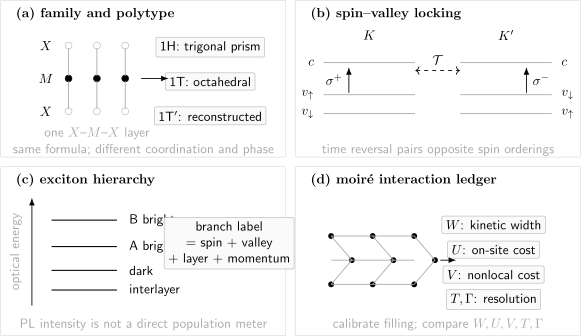
Four ledgers that must remain connected. (a) An –– monolayer does not by itself specify 1H, 1T, or a reconstructed polytype. (b) Broken inversion and spin–orbit coupling pair opposite spin orderings at and while time reversal preserves Kramers partners. (c) Optical spectra contain bright, dark, A/B, and interlayer excitations rather than one universal “exciton.” (d) A TMD moiré band is diagnosed by comparing bandwidth , on-site interaction , longer-range interaction , temperature, and disorder.
Valley ordering is material and thickness dependent
Section titled “Valley ordering is material and thickness dependent”For common semiconducting group-VI monolayers, the lowest direct optical transitions occur near and . The valence edge there is dominated by metal and combinations, while the conduction edge has substantial character. This orbital content explains why spin–orbit splitting is generally much larger in the valence sector than in the simplest conduction sector.
The statement “a TMD monolayer has a direct gap” is not a theorem for every . Even within the familiar compounds, nearby extrema at and the six valleys affect transport, high doping, strain response, and multilayer crossover. Layer number changes hybridization differently at , , and , and can move the fundamental gap away from the optically bright valley. A calculation or experiment should therefore report both the momentum of each edge and whether the quoted gap is quasiparticle, optical, or a density-dependent transport scale.
Monolayer Valley Hamiltonian
Section titled “Monolayer Valley Hamiltonian”A two-band model fixes the leading convention
Section titled “A two-band model fixes the leading convention”Let label and , let denote the approximately out-of-plane spin, and let be momentum measured from the chosen valley. In a common basis of conduction- and valence-edge orbitals, a minimal model is
Here is a lattice-length convention, controls interband velocity, is the gap parameter before the displayed spin splitting, and is the valence-edge splitting in this model. The Pauli matrices act in the two-orbital band-edge basis, not on real spin.
The eigenvalues are
At ,
Thus the model gives a spin-independent conduction edge and a valence splitting at fixed valley. Real materials have a finite, material-dependent conduction splitting generated by remote bands and additional spin–orbit terms. Quantitative models may also need electron–hole asymmetry, trigonal warping, valleys, strain, dielectric self-energy, and multiple orbitals. The two-band Hamiltonian is a symmetry-organized baseline, not a universal parameter table.
Time reversal locks spin to valley without polarizing equilibrium
Section titled “Time reversal locks spin to valley without polarizing equilibrium”Time reversal reverses momentum and spin. With the above local valley coordinates,
The upper valence state at therefore has the opposite spin to its degenerate partner at . This is spin–valley locking. It suppresses some elastic intervalley processes because changing valley can require changing spin, but it does not create a net equilibrium spin or valley polarization: the time-reversed partners are equally occupied unless a preparation, field, interaction, or boundary selects them.
Circularly polarized light can address opposite valleys near the band edge. In one common convention, couples most strongly at one valley and at the other; reversing the valley or helicity convention swaps those labels. The invariant statement is about the dipole matrix elements,
and their valley contrast. A helicity-resolved peak demonstrates a selection-rule-weighted optical response, not by itself a long-lived population, a dc valley current, or a topological invariant.
Spin–Orbit and Valley Response
Section titled “Spin–Orbit and Valley Response”A and B transitions are not a bare spin–orbit meter
Section titled “A and B transitions are not a bare spin–orbit meter”The large valence splitting creates two prominent direct exciton families. The A exciton is built mainly from the upper spin-split valence band and the relevant conduction edge; the B exciton begins from the lower valence band. Schematically,
Their separation is therefore
It is related to valence spin–orbit splitting, but it need not equal the bare splitting. Conduction-band spin structure, different reduced masses, exchange, screening, and band-dependent self-energy corrections all contribute. Extracting an atomic spin–orbit constant from the A–B peak spacing alone is therefore overconfident.
The sign of the small conduction splitting controls whether the lowest intravalley exciton is spin-allowed or spin-forbidden. Tungsten-based and molybdenum-based compounds often have different bright–dark orderings, but the rule is not universal across dielectric environments, strain, density, layer configuration, and momentum-indirect states. State the compound and the ordering actually inferred.
Magnetic shifts combine several moments
Section titled “Magnetic shifts combine several moments”For a specified exciton branch, a small out-of-plane field is often summarized by
where the sign depends on how the two helicities or valleys are subtracted. The effective can contain spin, atomic-orbital, Berry-curvature, and cyclotron contributions from both electron and hole. It may also vary with exciton character, hybridization, and moiré registry.
A measured linear splitting is valuable, but “” is not a complete microscopic interpretation. Record the branch, field orientation, polarization convention, fitting range, and whether means or the reverse. Diamagnetic shifts, field-induced brightening, and exchange with resident carriers can enter beyond the simplest linear regime.
Exciton Hierarchy
Section titled “Exciton Hierarchy”Coulomb physics dominates the optical threshold
Section titled “Coulomb physics dominates the optical threshold”Reduced screening makes neutral electron–hole pairs prominent in monolayer spectra. The generic relation
is developed, together with nonlocal screening, on Two-Dimensional Materials. In a TMD, however, belongs to a branch carrying valley, spin, center-of-mass momentum, and orbital composition. The branch labels are part of the observable.
| excitation | defining content | typical access | common overclaim |
|---|---|---|---|
| A or B exciton | electron and hole from specified spin-split valley bands | absorption, reflectance, photoluminescence | A–B spacing equals bare atomic spin–orbit splitting |
| spin-dark exciton | intravalley pair with suppressed spin-allowed dipole | magnetic brightening, phonon sidebands, time-resolved probes | weak PL means low population |
| momentum-indirect exciton | electron and hole at different valleys or momenta | phonon-assisted or momentum-sensitive spectroscopy | every low-energy shoulder is a dark exciton |
| trion or exciton polaron | optical excitation coupled to resident charge | density-dependent absorption and many-body line-shape analysis | every charged branch is an isolated three-body trion |
| biexciton or higher complex | correlated state involving multiple pairs | nonlinear and density-dependent optics | superlinear PL uniquely identifies a biexciton |
| interlayer exciton | electron and hole concentrated in different layers | Stark shift, lifetime, layer-sensitive and polarization probes | low energy alone proves layer separation |
Photoluminescence intensity depends on preparation, relaxation, light-cone occupation, nonradiative loss, collection, and matrix element. It is neither a direct population meter nor a binding-energy measurement. A neutral-exciton binding energy requires a quasiparticle gap from an independent or jointly constrained probe, not merely the separation between a PL peak and an assumed band edge.
At finite carrier density, an optical excitation interacts with a Fermi sea. The attractive and repulsive exciton-polaron branches can be more faithful than an isolated three-particle trion picture. Which language is useful depends on density, Fermi energy, disorder, and the spectral observable; a peak label should not be promoted into a microscopic proof without its density evolution and oscillator-strength transfer.
Interlayer excitons add a dipole and a registry ledger
Section titled “Interlayer excitons add a dipole and a registry ledger”In a type-II heterobilayer, the conduction and valence edges can favor different layers. An electron and hole then form an interlayer exciton with an out-of-plane electric dipole. To leading order, a displacement field produces
where is an effective charge-separation length rather than automatically the geometric layer spacing. Interlayer separation can lengthen radiative lifetime, but hybridization, momentum mismatch, moiré localization, defects, and nonradiative channels also matter.
A persuasive interlayer assignment combines several observations: a field-dependent Stark slope, layer-consistent band alignment, polarization and valley behavior, time-resolved dynamics, and reproducibility across spatial position and excitation power. Long lifetime alone is not unique because dark intralayer states and traps can also emit slowly.
Moiré Heterobilayers
Section titled “Moiré Heterobilayers”Mismatch and twist set a long geometric scale
Section titled “Mismatch and twist set a long geometric scale”Near parallel or antiparallel alignment, often called R-type and H-type stacking respectively, the local atomic registry varies slowly across a bilayer. Moiré Superlattices derives the generic period and triangular-cell area from lattice mismatch and twist. Applied to a TMD pair, that construction must use the measured lattice constants, local angle, and heterostrain rather than a nominal fabrication angle.
The density represents one particle per measured moiré cell. Converting a gate voltage into filling still requires geometric capacitance, quantum capacitance, trapped charge, contact behavior, and any parallel conducting channels.
The moiré modulation of a carrier valley can be organized as
where the shortest moiré reciprocal vectors are related by threefold rotation. Depending on material and stacking, the continuum Hamiltonian also needs layer-dependent dispersions, interlayer tunnelling, displacement-field offsets, spin–valley structure, and lattice relaxation.
For an exciton center of mass , a useful first reduction is
with inherited from the registry dependence of band edges, binding, and hybridization. Multiple moiré exciton peaks can arise from quantized confinement, minibands, or hybridized intra- and interlayer excitons. Similar peak multiplicity can also come from strain, domains, phonon replicas, charged complexes, or disorder. Twist-angle dependence, spatial maps, polarization, density, temperature, and power dependence are therefore part of the identification.
TMD narrow bands do not require a graphene magic-angle mechanism
Section titled “TMD narrow bands do not require a graphene magic-angle mechanism”In twisted graphene, velocity renormalization of coupled Dirac cones motivates a special dimensionless coupling and magic-angle language. TMD band edges are often massive, and their moiré potentials can be strongly registry dependent. Large effective mass, long moiré period, and local band-edge modulation can make the kinetic bandwidth small without tuning to a graphene-like velocity zero.
That distinction does not make the problem simple. Atomic relaxation can reconstruct the nominal sinusoidal pattern into stacking domains and solitons. Heterostrain changes local periods and symmetries. Remote valleys can approach the active band. A displacement field can change layer polarization and bandwidth. A faithful model must show that the retained bands are isolated over the parameter window and that its Wannier or continuum representation preserves their symmetry and topology.
Correlated Moiré Phases
Section titled “Correlated Moiré Phases”The extended Hubbard model is a hypothesis to validate
Section titled “The extended Hubbard model is a hypothesis to validate”When a narrow, isolated moiré band admits localized orbitals, a common starting point is
The label may represent spin–valley-locked flavor, layer, orbital, or a mixture; it should not automatically be read as bare spin. The effective lattice can be triangular, honeycomb, or multi-orbital depending on stacking and which valley manifold is active. Complex hopping phases and Berry curvature can obstruct a naive one-orbital description or make topology part of the low-energy ledger.
The useful hierarchy is not merely “ is large.” Compare
where is active-band width, a representative nonlocal interaction, the gap to omitted bands, and a disorder scale. A single-band Hubbard reduction requires over the operating range. Strong coupling requires interactions large relative to , while observing coherent low-energy order additionally requires temperature and inhomogeneity below the relevant collective scale.
Integer and fractional insulators require different audits
Section titled “Integer and fractional insulators require different audits”Insulation near one carrier per moiré cell can be consistent with Mott localization, but band gaps, flavor polarization, charge transfer, disorder, and symmetry breaking can also suppress transport. At fractional filling, longer-range repulsion can stabilize generalized Wigner crystals or other charge-ordered states. The commensurate filling is evidence for a moiré origin, not a complete phase diagnosis.
| observation | supports | still needed |
|---|---|---|
| resistance peak at integer | incompressible or poorly conducting regime tied to filling | contact audit, activation or nonlinear transport, compressibility |
| optical anomaly at rational | coupling between an optical sensor and resident correlated carriers | independent density calibration and charge-sensitive probe |
| reduced compressibility | thermodynamic incompressibility | disorder and geometric-capacitance subtraction |
| magnetic circular dichroism or anomalous Hall response | flavor or orbital magnetism | hysteresis, domain, contact, and zero-field controls |
| fractional-filling sequence | importance of nonlocal interaction and commensurability | real-space pattern, symmetry, and competing-state comparison |
Optical sensing is powerful because a TMD exciton responds to local charge and spin correlations, but it is indirect. Combining it with transport, capacitance or compressibility, local microwave impedance, spatial imaging, and magnetic response separates a spectroscopic marker from a thermodynamic phase claim.
Experiments in WSe/WS heterobilayers have reported integer and fractional correlated insulating states, while twisted WSe homobilayers have enabled displacement-field-tuned metal–insulator transitions and quantum-critical transport. These results establish a highly tunable interacting platform. They do not imply that every device realizes the same one-band Hamiltonian: twist angle, R- versus H-type stacking, layer polarization, contacts, and remote valleys vary across experiments.
Superconductivity is established experimentally; its mechanism is active
Section titled “Superconductivity is established experimentally; its mechanism is active”Two 2025 reports observed superconducting transport in twisted bilayer WSe at different twist angles, and later twist-angle studies mapped superconducting domes adjacent to bandwidth-tuned correlated regimes. The experimental claim of superconductivity is supported by resistance drops or zero-resistance regions, current dependence, field suppression, and transition analyses within the reported devices. That is stronger than a lone resistance downturn.
The pairing mechanism, gap representation, role of spin–valley locking, and relation to nearby magnetism, strange-metal behavior, or a Mott transition remain active research. A triangular-lattice Hubbard model, longer-range interactions, phonons, and band geometry provide candidate ingredients; none should be presented as the settled explanation. BCS Theory supplies the conventional benchmark, Quantum Criticality supplies the scaling standards, and Strange Metals supplies the transport audit.
Finally, do not conflate these carrier-doped semiconducting moiré phases with intrinsic charge order and superconductivity in metallic NbSe, TaS, or related compounds. They share the TMD chemical label but begin from different bands, Fermi surfaces, ordering tendencies, and effective models.
Experimental Claim Ladder
Section titled “Experimental Claim Ladder”- Establish the specimen. Determine composition, polytype, layer count, twist, strain, domains, encapsulation, contacts, and gate geometry.
- Calibrate single-particle structure. Identify relevant , , and edges; resolve layer and spin character where possible.
- Assign optical branches. Use polarization, field, density, temperature, power, and lifetime together rather than naming peaks by energy alone.
- Calibrate moiré filling. Cross-check cell area, Hall or capacitance density, neutrality offsets, and spatial inhomogeneity.
- Demonstrate a phase property. Use transport, compressibility, symmetry response, spatial order, or collective behavior appropriate to the claim.
- Test alternatives. Compare band insulation, disorder, traps, reconstruction, charge transfer, and competing orders before assigning a many-body label.
- Report frontier status. Separate observed behavior from the effective model and from the proposed microscopic mechanism.
Common Mistakes
Section titled “Common Mistakes”Treating TMD as a synonym for monolayer MoS₂
Section titled “Treating TMD as a synonym for monolayer MoS₂”The family spans semiconductors, metals, reconstructed phases, magnets, charge-ordered compounds, and superconductors. Composition, polytype, and thickness belong in the first sentence of a claim.
Calling every spin splitting Rashba coupling
Section titled “Calling every spin splitting Rashba coupling”The leading monolayer valley splitting follows from atomic spin–orbit coupling and crystal symmetry. Rashba terms require the appropriate inversion asymmetry and have a distinct momentum and spin texture.
Reading population directly from photoluminescence
Section titled “Reading population directly from photoluminescence”PL weights occupation by radiative access and competes with nonradiative loss. A dark state can be highly populated and weakly emissive; a bright line can have strong oscillator strength without dominating the total population.
Equating an optical gap with a band gap
Section titled “Equating an optical gap with a band gap”The optical threshold includes electron–hole binding and many-body renormalization. State whether a value is quasiparticle, optical, transport, or model-derived.
Inferring a moiré exciton from a multiplet alone
Section titled “Inferring a moiré exciton from a multiplet alone”Strain, disorder, phonons, charged complexes, and domains also create multiple lines. Moiré assignment needs geometry- and control-dependent evidence.
Calling every commensurate insulator a Mott state
Section titled “Calling every commensurate insulator a Mott state”Band reconstruction, flavor order, charge transfer, generalized Wigner order, and disorder can all matter. The model and phase need separate validation.
Exercises
Section titled “Exercises”Exercise 1: band-edge splitting in the minimal model
Section titled “Exercise 1: band-edge splitting in the minimal model”Set in the two-band Hamiltonian. Find the conduction and valence energies and show that the valence splitting at fixed is . Why does this not predict the full experimental A–B exciton separation?
Solution
At , the conduction basis state has , so the spin–orbit projector vanishes:
The valence basis state has , giving
At fixed valley, changing from to changes the valence energy by magnitude
The A and B optical lines are excitons, not bare interband gaps. Their separation also contains conduction splitting, branch-dependent binding, exchange, effective masses, and quasiparticle self-energy corrections. Therefore it need not equal .
Exercise 2: time reversal and spin–valley locking
Section titled “Exercise 2: time reversal and spin–valley locking”For the displayed spectrum, verify . Explain why spin–valley locking does not imply equilibrium magnetization.
Solution
The spectrum depends on and on the product . Under
both and remain unchanged, so the energies agree. The highest valence state at one valley is paired with an opposite-spin state at the other valley.
In equilibrium with time-reversal symmetry, the two partners have equal energy and equal statistical occupation. Their spin and orbital moments cancel when summed over valleys. A net magnetization requires unequal occupation or spontaneous time-reversal breaking, not merely spin–valley correlation.
Exercise 3: why the A–B spacing is not a bare constant
Section titled “Exercise 3: why the A–B spacing is not a bare constant”Let the two quasiparticle gaps be and the two binding energies differ by . Express the optical A–B separation. Evaluate it for and .
Solution
Using ,
Even in this simplified example, the optical separation differs from the quasiparticle valence contribution by . Additional conduction, exchange, and self-energy terms can alter it further.
Exercise 4: moiré period and one-particle density
Section titled “Exercise 4: moiré period and one-particle density”Take , lattice mismatch , and twist . Estimate , , and the density for one particle per moiré cell.
Solution
First convert the angle to radians:
Then
The triangular-cell area is
Since ,
This is a geometric estimate. A voltage-to-filling conversion still needs a device capacitance and offset calibration.
Exercise 5: valley Zeeman scale
Section titled “Exercise 5: valley Zeeman scale”An exciton branch has under the convention . Estimate the signed splitting at using .
Solution
The magnitude is . The minus sign says that under the stated subtraction convention; changing the helicity convention would change the reported sign.
Exercise 6: audit a correlated-insulator claim
Section titled “Exercise 6: audit a correlated-insulator claim”A WSe/WS device shows a resistance maximum and an exciton-energy kink at a gate voltage assigned to . The authors call the state a generalized Wigner crystal. List four checks that would materially strengthen or weaken that interpretation.
Solution
Useful checks include:
- independently calibrate density and moiré-cell area, including trapped charge and spatial twist variation;
- measure compressibility or capacitance to test thermodynamic incompressibility rather than contact-limited resistance;
- map nearby rational fillings and temperature scales to test a systematic commensurability sequence;
- use a spatial or symmetry-sensitive probe to seek the predicted charge pattern or broken lattice symmetry;
- vary displacement field and dielectric screening to test the expected balance of ;
- rule out ordinary localization, traps, parallel channels, and an accidental single-particle minigap.
The resistance and optical anomalies establish a reproducible filling-linked state. They do not alone determine its microscopic charge pattern.
Key Takeaways
Section titled “Key Takeaways”- identifies a chemical family; polytype, layer count, and stacking determine which low-energy theory applies.
- A minimal group-VI monolayer model couples valley, orbital pseudospin, and real spin, giving opposite spin orderings at time-reversed valleys.
- Valley-selective optical coupling is a matrix-element statement, not automatic proof of a valley population or topological phase.
- TMD optical spectra are dominated by a branch-dependent exciton hierarchy; optical and quasiparticle gaps must remain separate.
- TMD moiré bands can become narrow through massive band edges and registry potentials without a graphene-like magic-angle mechanism.
- Correlated insulators and superconductivity are experimentally established in selected TMD moiré devices, while microscopic phase assignments and pairing mechanisms remain active.
Connections
Section titled “Connections”- Two-Dimensional Materials develops generic screening, exciton-gap bookkeeping, heterostructures, and device electrostatics.
- van der Waals Heterostructures owns stack assembly, rotational alignment, encapsulation, contacts, proximity channels, and vertical-device diagnostics.
- Moiré Superlattices owns reciprocal mismatch, cell and filling conversion, mini-zone construction, generic flattening mechanisms, and simulator validation.
- Correlated Insulators in Moiré Systems distinguishes TMD Mott-like states, generalized Wigner charge order, flavor structure, and thermodynamic evidence.
- Moiré Superconductivity compares TMD and graphene moiré condensates through gate tuning, BKT stiffness, spin–valley pairing constraints, and mechanism tests.
- Moiré Topology develops spin–valley Chern bands, QAH evidence, fractional Chern states, and the role of layer-pseudospin texture.
- Low-Dimensional Quantum Matter distinguishes geometric confinement from a demonstrated low-dimensional regime.
- Band Theory Overview supplies the quasiparticle and Bloch-band baseline.
- Spin–Orbit Coupling in Solids owns symmetry-allowed spin textures and microscopic spin–orbit mechanisms.
- 2D Magnets and Ferroelectrics develops magnetic-proximity valley response, sliding TMD ferroelectricity, and coupled spin–valley–lattice order.
- Berry Curvature develops the local band geometry behind valley orbital response.
- Chern Numbers in Band Theory explains when valley-resolved curvature can be promoted to a global invariant.
- Hubbard Physics in Materials supplies the validation chain from bands to interacting lattice models.
- Mott Insulators separates interaction-driven incompressibility from a resistance maximum alone.
- Charge and Spin Density Waves owns metallic-TMD charge order and finite-wavevector diagnostics.
- BCS Theory is the conventional pairing benchmark for interpreting moiré superconductivity.
- Quantum Criticality and Strange Metals provide the scaling and transport standards for frontier claims.
Further Reading
Section titled “Further Reading”- G. Wang et al., “Colloquium: Excitons in Atomically Thin Transition Metal Dichalcogenides,” Reviews of Modern Physics 90, 021001 (2018), doi:10.1103/RevModPhys.90.021001.
- A. Kormányos et al., “ Theory for Two-Dimensional Transition Metal Dichalcogenide Semiconductors,” 2D Materials 2, 022001 (2015), doi:10.1088/2053-1583/2/2/022001.
- S. Manzeli, D. Ovchinnikov, D. Pasquier, O. V. Yazyev, and A. Kis, “2D Transition Metal Dichalcogenides,” Nature Reviews Materials 2, 17033 (2017), doi:10.1038/natrevmats.2017.33.
References
Section titled “References”- K. F. Mak, C. Lee, J. Hone, J. Shan, and T. F. Heinz, “Atomically Thin MoS: A New Direct-Gap Semiconductor,” Physical Review Letters 105, 136805 (2010), doi:10.1103/PhysRevLett.105.136805.
- A. Splendiani et al., “Emerging Photoluminescence in Monolayer MoS,” Nano Letters 10, 1271–1275 (2010), doi:10.1021/nl903868w.
- D. Xiao, G.-B. Liu, W. Feng, X. Xu, and W. Yao, “Coupled Spin and Valley Physics in Monolayers of MoS and Other Group-VI Dichalcogenides,” Physical Review Letters 108, 196802 (2012), doi:10.1103/PhysRevLett.108.196802.
- T. Cao et al., “Valley-Selective Circular Dichroism of Monolayer Molybdenum Disulphide,” Nature Communications 3, 887 (2012), doi:10.1038/ncomms1882.
- K. F. Mak, K. He, J. Shan, and T. F. Heinz, “Control of Valley Polarization in Monolayer MoS by Optical Helicity,” Nature Nanotechnology 7, 494–498 (2012), doi:10.1038/nnano.2012.96.
- T. C. Berkelbach, M. S. Hybertsen, and D. R. Reichman, “Theory of Neutral and Charged Excitons in Monolayer Transition Metal Dichalcogenides,” Physical Review B 88, 045318 (2013), doi:10.1103/PhysRevB.88.045318.
- A. Chernikov et al., “Exciton Binding Energy and Nonhydrogenic Rydberg Series in Monolayer WS,” Physical Review Letters 113, 076802 (2014), doi:10.1103/PhysRevLett.113.076802.
- J. S. Ross et al., “Electrical Control of Neutral and Charged Excitons in a Monolayer Semiconductor,” Nature Communications 4, 1474 (2013), doi:10.1038/ncomms2498.
- P. Rivera et al., “Observation of Long-Lived Interlayer Excitons in Monolayer MoSe–WSe Heterostructures,” Nature Communications 6, 6242 (2015), doi:10.1038/ncomms7242.
- H. Yu, G.-B. Liu, J. Tang, X. Xu, and W. Yao, “Moiré Excitons: From Programmable Quantum Emitter Arrays to Spin-Orbit-Coupled Artificial Lattices,” Science Advances 3, e1701696 (2017), doi:10.1126/sciadv.1701696.
- E. M. Alexeev et al., “Resonantly Hybridized Excitons in Moiré Superlattices in van der Waals Heterostructures,” Nature 567, 81–86 (2019), doi:10.1038/s41586-019-0986-9.
- K. L. Seyler et al., “Signatures of Moiré-Trapped Valley Excitons in MoSe/WSe Heterobilayers,” Nature 567, 66–70 (2019), doi:10.1038/s41586-019-0957-1.
- K. Tran et al., “Evidence for Moiré Excitons in van der Waals Heterostructures,” Nature 567, 71–75 (2019), doi:10.1038/s41586-019-0975-z.
- C. Jin et al., “Observation of Moiré Excitons in WSe/WS Heterostructure Superlattices,” Nature 567, 76–80 (2019), doi:10.1038/s41586-019-0976-y.
- F. Wu, T. Lovorn, E. Tutuc, and A. H. MacDonald, “Hubbard Model Physics in Transition Metal Dichalcogenide Moiré Bands,” Physical Review Letters 121, 026402 (2018), doi:10.1103/PhysRevLett.121.026402.
- Y. Tang et al., “Simulation of Hubbard Model Physics in WSe/WS Moiré Superlattices,” Nature 579, 353–358 (2020), doi:10.1038/s41586-020-2085-3.
- E. C. Regan et al., “Mott and Generalized Wigner Crystal States in WSe/WS Moiré Superlattices,” Nature 579, 359–363 (2020), doi:10.1038/s41586-020-2092-4.
- Y. Xu et al., “Correlated Insulating States at Fractional Fillings of Moiré Superlattices,” Nature 587, 214–218 (2020), doi:10.1038/s41586-020-2868-6.
- X. Huang et al., “Correlated Insulating States at Fractional Fillings of the WS/WSe Moiré Lattice,” Nature Physics 17, 715–719 (2021), doi:10.1038/s41567-021-01171-w.
- T. Li et al., “Continuous Mott Transition in Semiconductor Moiré Superlattices,” Nature 597, 350–354 (2021), doi:10.1038/s41586-021-03853-0.
- A. Ghiotto et al., “Quantum Criticality in Twisted Transition Metal Dichalcogenides,” Nature 597, 345–349 (2021), doi:10.1038/s41586-021-03815-6.
- Y. Guo et al., “Superconductivity in 5.0° Twisted Bilayer WSe,” Nature 637, 839–845 (2025), doi:10.1038/s41586-024-08381-1.
- Y. Xia et al., “Superconductivity in Twisted Bilayer WSe,” Nature 637, 833–838 (2025), doi:10.1038/s41586-024-08116-2.
- Y. Xia et al., “Bandwidth-Tuned Mott Transition and Superconductivity in Moiré WSe,” Nature 650, 585–591 (2026), doi:10.1038/s41586-025-10049-3.