Two-Dimensional Materials
A two-dimensional material is a crystalline sheet whose electronically and mechanically relevant thickness is one or a few atomic layers. Its carriers may be kinematically two dimensional, but its electric fields, photons, substrate modes, and contacts generally inhabit a three-dimensional environment. That mixed-dimensional character is responsible for much of the subject’s distinctive physics.
The phrase names a platform class, not one band structure or phase. Graphene is a gapless Dirac semimetal; hexagonal boron nitride is a wide-gap insulator; many transition-metal dichalcogenide monolayers are semiconductors; other layered compounds can be metallic, magnetic, ferroelectric, or superconducting. Layer count, stacking, strain, encapsulation, dielectric environment, contacts, and gate configuration can all change the measured system.
A trustworthy analysis keeps six ledgers together:
- atomic structure and layer number;
- quasiparticle bands and symmetry;
- nonlocal dielectric screening;
- neutral and charged optical excitations;
- interfaces, twist, and proximity coupling;
- electrostatic control, disorder, and contacts.
Canonical Scope
Section titled “Canonical Scope”This page is the canonical home for atomically thin crystals as a materials platform. It owns the distinction between a monolayer crystal and an interface-confined electron gas, membrane stability, environmental screening, and the platform-level valley, exciton, stacking, and device-control ledgers.
Low-Dimensional Quantum Matter owns the general definition of effective dimension, dimensional state counting, fluctuation constraints, and crossover evidence. van der Waals Heterostructures owns layer-sequence design, interface cleanliness, rotational alignment, encapsulation, gate architecture, proximity channels, and vertical-device evidence. Graphene and Dirac Materials owns graphene’s honeycomb Hamiltonian, pseudospin, Berry phase, and Landau levels. Two-Dimensional Electron Gases owns populated semiconductor and oxide interfaces. Random Phase Approximation owns self-consistent polarization, dielectric response, and bubble resummation.
The exciton model below is used to explain why optical and quasiparticle gaps differ in an atomically thin semiconductor. It does not replace a general theory of Wannier–Mott, Frenkel, charge-transfer, or strongly correlated excitons.
Monolayer Crystals
Section titled “Monolayer Crystals”Layered bonding creates an exfoliation plane
Section titled “Layered bonding creates an exfoliation plane”Many atomically thin crystals descend from three-dimensional parent compounds with strong in-plane bonding and weaker interlayer adhesion. Mechanical or liquid exfoliation separates layers; chemical vapor deposition, epitaxy, and other growth methods can instead form sheets directly. “Van der Waals material” usually describes the weakly bonded stacking direction, not the absence of covalent or ionic bonds inside a layer.
A monolayer may contain more than one atomic plane. Monolayer MoS₂, for example, is an S–Mo–S trilayer in atomic structure but one electronically coherent layer. The physically relevant layer count must therefore be tied to a crystallographic repeat unit, not to a casual count of visible planes.
| Representative family | Low-energy character | Structural caution |
|---|---|---|
| graphene and related honeycomb sheets | Dirac or reconstructed semimetal | substrate and alignment can break sublattice symmetry |
| hexagonal boron nitride | wide-gap polar insulator | often functions as substrate, spacer, or tunnel barrier |
| transition-metal dichalcogenides | semiconductor, metal, charge order, or superconductor | polytype and layer parity change symmetry |
| black phosphorus and related puckered layers | anisotropic semiconductor | oxidation and crystal-axis assignment matter |
| magnetic or ferroelectric layers | symmetry-broken insulating or semiconducting states | anisotropy, domains, and finite size control apparent order |
This table is a taxonomy, not a material-property database. Phase, gap, mobility, and stability values depend strongly on preparation and environment.
A crystal can be flat without being perfectly planar
Section titled “A crystal can be flat without being perfectly planar”For an elastic membrane with out-of-plane displacement , a harmonic free energy contains bending and tension,
where is bending rigidity and is tension. With areal mass density , the flexural dispersion is
For a tensionless harmonic membrane, thermal height fluctuations obey
which is strongly infrared sensitive. This does not imply that atomically thin crystals cannot exist. In a crystalline membrane, nonlinear coupling between bending and in-plane strain renormalizes the long-wavelength elasticity; finite size, tension, substrate pinning, and microscopic corrugation also matter. Suspended graphene is experimentally corrugated rather than an ideal mathematical plane.
The absence of conventional translational long-range order in an ideal infinite two-dimensional crystal is therefore compatible with robust finite membranes and quasi-long-range crystalline correlations. It is another reason to distinguish a theorem’s thermodynamic assumptions from a laboratory specimen.
Removing a layer can change the band structure
Section titled “Removing a layer can change the band structure”Layer reduction changes more than confinement energy. It can remove inversion symmetry, alter orbital hybridization, change dielectric self-energy, and move different valleys by unequal amounts. A familiar example is the indirect-to-direct optical crossover of MoS₂ at monolayer thickness. The conclusion is material specific: monolayer formation does not generically make a semiconductor direct gap.
Band labels should state whether they refer to:
- a density-functional or quasiparticle calculation;
- a neutral optical transition;
- a tunnelling or photoemission threshold;
- an isolated sheet or a particular dielectric stack;
- a specified strain, doping, temperature, and layer registry.
Reduced and Nonlocal Screening
Section titled “Reduced and Nonlocal Screening”Fields escape the sheet
Section titled “Fields escape the sheet”In a bulk isotropic insulator, long-wavelength electrostatics is often summarized by one dielectric constant. In an atomically thin layer, electric field lines extend into the media above and below the sheet. Screening is therefore nonlocal and environmentally tunable.
For an isotropic polarizable sheet between media with relative permittivities and , define
A useful Rytova–Keldysh model for the repulsive interaction between unit charges is
where is a screening length proportional to the sheet polarizability. Definitions of the two-dimensional polarizability differ between SI and Gaussian conventions, so should be quoted directly or derived with the convention stated.
Writing , the corresponding real-space asymptotes are
At short distance the potential is approximately logarithmic; at long distance the field sees the surrounding dielectric and returns to a tail. This nonhydrogenic crossover is central to impurity states and excitons in semiconducting monolayers.
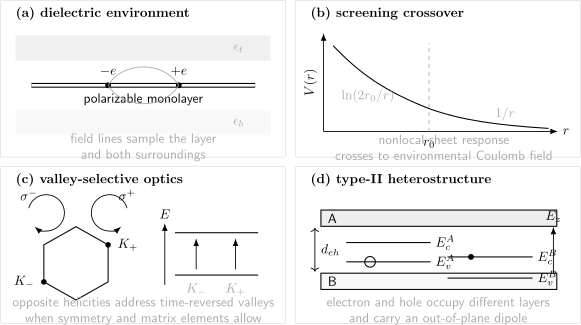
Four linked ledgers for a semiconducting monolayer: the fields sample both dielectric surroundings; the screened interaction crosses near ; time-reversed valleys can couple to opposite optical helicities; and a type-II stack can separate an electron and hole into different layers, creating an electrically tunable interlayer exciton.
The model has a domain of validity
Section titled “The model has a domain of validity”The Rytova–Keldysh form assumes a thin, approximately isotropic, local sheet polarizability and simple surrounding dielectrics. It must be refined for anisotropic layers, multilayers, metallic screening, free carriers, finite frequency, spatially dispersive substrates, nearby gates, and microscopic distances comparable to the lattice constant.
An ideal metallic gate a distance away can suppress the long-range interaction. In a simple homogeneous image-charge geometry,
This factor is not universal to every stack, but it shows why gate distance is part of the interaction Hamiltonian rather than only a device detail. Dynamic collective charge response belongs with Plasmons Preview, while carrier screening beyond this electrostatic model requires a polarization calculation.
Valley Degrees of Freedom
Section titled “Valley Degrees of Freedom”A valley is a momentum-space label
Section titled “A valley is a momentum-space label”A valley is a well-separated local extremum or low-energy pocket in momentum space. If two extrema at and are symmetry related, a label can act as a low-energy pseudospin. The label is useful only when intervalley scattering is weak on the timescale of interest.
Time reversal relates opposite valleys. For a nonmagnetic spinful system,
where is Berry curvature. Equal occupation of time-reversed valleys can therefore cancel the net charge Hall response even while valley-resolved carriers deflect in opposite transverse directions.
Not every two-dimensional band has a useful valley degree of freedom. The extrema must be distinct, long lived, and experimentally addressable. Edge disorder, short-range defects, phonons, exchange, and Coulomb scattering can transfer the large momentum needed to relax valley polarization.
Circular selection is a matrix-element statement
Section titled “Circular selection is a matrix-element statement”For light incident normal to a layer, define circular interband matrix elements
A local circular dichroism measure is
Broken inversion symmetry and orbital angular momentum can make have opposite signs in time-reversed valleys, as in idealized monolayer group-VI dichalcogenides. Spin–orbit coupling can further lock spin and valley labels near a band edge.
Circularly polarized photoluminescence is not by itself a direct population meter. Excitation detuning, exciton formation, exchange-driven depolarization, dark states, reabsorption, and polarization-dependent collection can all affect the measured helicity. A valley claim should combine selection rules with dynamics and at least one control that reverses the expected sign.
Excitons and Optical Gaps
Section titled “Excitons and Optical Gaps”Optical and quasiparticle gaps are different
Section titled “Optical and quasiparticle gaps are different”An electron promoted across a semiconductor gap leaves a hole. Their attraction can bind an exciton with relative-coordinate equation
where and denotes the magnitude of the attraction. The neutral exciton transition is approximately
before phonon, exchange, disorder, and many-body shifts are included. Here is the charged-particle addition–removal gap, not a Kohn–Sham eigenvalue difference.
For an ideal strictly two-dimensional interaction, the hydrogenic benchmark is
with
The ground-state binding is , four times the three-dimensional hydrogenic benchmark with the same and dielectric constant. Real monolayers are generally nonhydrogenic because the interaction crosses between logarithmic and Coulombic regimes, bands are not perfectly parabolic, and screening is frequency and environment dependent.
Spectra contain an exciton hierarchy
Section titled “Spectra contain an exciton hierarchy”An optical spectrum can include:
- bright intralayer excitons allowed by spin, momentum, and polarization selection rules;
- spin- or momentum-dark excitons;
- charged excitons or attractive exciton-polarons in a doped Fermi sea;
- biexcitons and other few-body complexes;
- interlayer excitons with electron and hole in different sheets;
- phonon sidebands, defect-bound states, and disorder-localized emission.
Peak assignment requires more than matching an energy. Useful controls include gate dependence, power dependence, polarization, magnetic field, temperature, lifetime, absorption or reflectance contrast, two-photon selection, and comparison with a separately measured quasiparticle continuum.
A photoluminescence peak alone does not determine the exciton binding energy. A binding-energy extraction needs both a neutral resonance and a defensible charged-particle continuum or Rydberg-series model. Chernikov and collaborators’ observation of a nonhydrogenic WS₂ Rydberg series is a canonical example of why the screening model matters.
Van der Waals Heterostructures
Section titled “Van der Waals Heterostructures”Stacking creates a new Hamiltonian
Section titled “Stacking creates a new Hamiltonian”Weak interlayer adhesion allows sheets with different lattice constants and chemistry to be assembled without the strict lattice matching demanded by conventional epitaxy. The layers can retain recognizable bands while acquiring tunnelling, electrostatic coupling, strain, and proximity interactions.
| Alignment | Band-edge arrangement | Typical low-energy consequence |
|---|---|---|
| type I | electron and hole edges favor the same layer | intralayer localization and emission |
| type II | electron and hole edges favor different layers | charge transfer and interlayer excitons |
| type III | conduction and valence edges overlap across layers | interband tunnelling and semimetallic reconstruction |
These labels describe a single-particle starting point. Hybridization, quasiparticle self-energy, interface dipoles, doping, strain, and exciton binding can revise the effective alignment.
For an interlayer exciton with charge separation , the out-of-plane dipole is approximately
Its leading Stark shift is
with sign fixed by the dipole orientation. Gate-tunable interlayer photoluminescence is useful evidence, but it should be combined with layer-resolved band alignment, excitation resonance, lifetime, and field-direction controls.
Clean interfaces are an experimental achievement
Section titled “Clean interfaces are an experimental achievement”Van der Waals assembly avoids many dangling bonds, but it does not guarantee an ideal interface. Trapped contamination can form bubbles; wrinkles and tears create strain; polymer residue dopes the layers; rotational and translational registry vary; and edge contacts can introduce disorder. Hexagonal boron nitride encapsulation often reduces charge inhomogeneity and supplies a flatter dielectric environment, but even encapsulated devices need a measured disorder and contact ledger.
Twist and lattice mismatch generate long-period moiré structure. Moiré Superlattices owns the reciprocal construction, mini Brillouin zones, minibands, interaction scales, and inhomogeneity analysis; a visible moiré pattern alone does not prove flat bands or correlated phases.
Device Control
Section titled “Device Control”Gate voltage is not identical to carrier density
Section titled “Gate voltage is not identical to carrier density”For a simple gate with geometric capacitance per area , a small voltage change divides between electrostatics and chemical potential:
The electronic compressibility defines the quantum capacitance
For an ideal series combination,
The common estimate is reliable only when quantum capacitance, trap charging, leakage, contact potential, and additional gates are negligible or independently calibrated.
Dual gates separate density and displacement
Section titled “Dual gates separate density and displacement”With top and bottom capacitances and , one convenient convention is
Here has units of surface charge density; some authors divide by or reverse a sign. The convention must be stated. Independent density and displacement control is especially valuable in bilayers and heterostructures, where a transverse field can shift layer polarization or band alignment.
Control knobs and their confounders
Section titled “Control knobs and their confounders”| Control | Primary action | Frequent confounder |
|---|---|---|
| electrostatic gate | density and chemical potential | traps, leakage, quantum capacitance |
| displacement field | layer polarization and band alignment | density cross-coupling |
| dielectric stack | interaction and disorder environment | remote phonons and strain |
| uniaxial or biaxial strain | symmetry and valley energies | gradients, slippage, cracks |
| optical pump | populations and coherent polarization | heating and nonequilibrium screening |
| twist or registry | hybridization and moiré period | spatial inhomogeneity |
| contacts | injection and electrochemical boundary conditions | Schottky barriers and contact doping |
A successful device interpretation closes this control matrix with independent density, temperature, leakage, contact, and spatial-homogeneity measurements.
Evidence Workflow
Section titled “Evidence Workflow”- Establish layer number and structure. Combine microscopy or diffraction with Raman, photoluminescence, or other calibrated thickness markers.
- State the dielectric and contact environment. Include substrate, encapsulation, gates, spacers, residues, and exposed surfaces.
- Separate quasiparticle and optical quantities. Name whether each energy comes from transport, tunnelling, photoemission, absorption, reflectance, or luminescence.
- Test symmetry assignments. Reverse helicity, field, crystal orientation, or layer parity as appropriate.
- Close the electrostatics. Calibrate density, displacement, quantum capacitance, traps, and leakage.
- Search for environmental response. Change dielectric thickness, gate distance, layer number, or encapsulation while tracking disorder.
- Report spatial variation. Bubbles, domains, strain, twist-angle disorder, and edge regions can dominate a local probe.
Common Mistakes
Section titled “Common Mistakes”- Treating every thin film as a two-dimensional material. An atomically thin crystal is distinct from a conventional film or interface-confined 2DEG.
- Using one bulk dielectric constant. Monolayer screening is generally nonlocal and depends on the surrounding stack.
- Calling every pair of extrema a robust valley pseudospin. Intervalley relaxation and experimental addressability must be demonstrated.
- Equating polarized luminescence with valley population. Optical matrix elements and relaxation enter the measured polarization.
- Reading the quasiparticle gap from photoluminescence. A neutral exciton peak is shifted below the charged-particle continuum.
- Fitting all excitons with a two-dimensional hydrogen series. Rytova–Keldysh screening removes the accidental hydrogenic pattern.
- Assuming a clean van der Waals interface. Contamination, strain, registry, and contacts need direct checks.
- Converting gate voltage directly to density. Quantum capacitance, traps, multiple gates, and leakage can invalidate the plate-capacitor estimate.
- Calling tunability a phase diagnosis. A gate-dependent feature still needs an operator-specific and symmetry-aware identification.
Exercises
Section titled “Exercises”Exercise 1: flexural fluctuation power counting
Section titled “Exercise 1: flexural fluctuation power counting”For a tensionless harmonic membrane, use to determine how depends on linear system size in two dimensions. What changes when finite tension dominates?
Solution
In two dimensions,
The infrared contribution scales as in the tensionless harmonic theory. If tension dominates, the denominator becomes , so
Real crystalline membranes require anharmonic coupling between bending and in-plane strain, which renormalizes this naive harmonic scaling.
Exercise 2: screening asymptotes
Section titled “Exercise 2: screening asymptotes”Explain from why the interaction approaches at and a logarithm at .
Solution
Large real-space distance samples small , where . Thus , whose two-dimensional Fourier transform is proportional to .
Short distance samples , where
The two-dimensional Fourier transform of is logarithmic. The crossover is smooth, and the continuum model ceases to be reliable once approaches the lattice scale.
Exercise 3: ideal two-dimensional exciton
Section titled “Exercise 3: ideal two-dimensional exciton”Compare the ideal two-dimensional and three-dimensional hydrogenic ground-state binding energies for the same reduced mass and dielectric constant. Give two reasons a monolayer semiconductor need not realize this ratio.
Solution
The three-dimensional ground state has . In two dimensions,
The ideal two-dimensional state is therefore four times more strongly bound. Real monolayers have nonlocal Rytova–Keldysh screening rather than a constant-dielectric interaction, and their bands can be nonparabolic or multivalley. Finite layer thickness, dielectric anisotropy, exchange, and dynamical screening provide additional corrections.
Exercise 4: time reversal and valley Hall cancellation
Section titled “Exercise 4: time reversal and valley Hall cancellation”Suppose two time-reversed valleys have equal carrier densities and opposite Berry curvature. Show why the net anomalous charge Hall conductivity cancels while a valley Hall current can remain.
Solution
The intrinsic contribution from one valley has schematic form
Time reversal gives . Equal occupations make
The difference, which weights opposite valleys with opposite signs, need not vanish. A net charge Hall signal requires valley imbalance, broken time reversal, or another asymmetry that prevents cancellation.
Exercise 5: quantum-capacitance limit
Section titled “Exercise 5: quantum-capacitance limit”Show that when and in the opposite limit. What does each regime measure?
Solution
From
the smaller series capacitance controls the result. If , then , making the measurement sensitive to thermodynamic density of states and compressibility. If , then , and ordinary electrostatics controls the gate conversion. Trap and stray capacitances must still be separated experimentally.
Exercise 6: interlayer-exciton Stark slope
Section titled “Exercise 6: interlayer-exciton Stark slope”An interlayer exciton has electron–hole separation . Estimate the magnitude of its linear energy shift per electric field of .
Solution
Using ,
Thus the ideal dipole estimate is . The measured slope can differ because the electron and hole wave functions are not point charges, dielectric screening and hybridization change with field, and the local field may differ from the externally quoted displacement field.
Key Takeaways
Section titled “Key Takeaways”- A two-dimensional material is an atomically thin crystal embedded in a generally three-dimensional electromagnetic and mechanical environment.
- Membrane fluctuations are infrared sensitive, but anharmonic elasticity, finite size, tension, corrugation, and substrates stabilize laboratory sheets.
- Monolayer screening is nonlocal; the Rytova–Keldysh length and surrounding dielectrics belong in the Hamiltonian.
- Valleys are symmetry- and lifetime-dependent momentum-space labels, not automatic properties of every two-dimensional band.
- Optical excitons lie below the quasiparticle gap and generally follow a nonhydrogenic spectrum in atomically thin semiconductors.
- Van der Waals stacking creates hybridization, proximity, band-alignment, and dipolar-exciton physics while retaining strong sensitivity to interface disorder.
- Gate voltage becomes a reliable density control only after geometric capacitance, quantum capacitance, traps, leakage, and multiple gates are closed.
Connections
Section titled “Connections”- Low-Dimensional Quantum Matter supplies the scale-dependent definition of effective dimension and crossover.
- Graphene and Dirac Materials develops the canonical gapless honeycomb example.
- Graphene develops the materials-engineering perturbation ledger, strain pseudogauge fields, Hall nomenclature, and moiré handoff.
- Transition-Metal Dichalcogenides specializes the platform ledger to polytypes, spin–valley locking, A/B and dark excitons, TMD moiré bands, and correlated-phase evidence.
- 2D Magnets and Ferroelectrics specializes the platform ledger to anisotropy, layer-parity magnetism, sheet polarization, sliding ferroelectricity, and magnetoelectric evidence.
- van der Waals Heterostructures develops stack assembly, alignment, contacts, gate architecture, proximity self-energies, and vertical tunneling.
- Moiré Superlattices develops the generic geometric, reciprocal-space, miniband, filling, and interaction hierarchy of moiré matter.
- Two-Dimensional Electron Gases distinguishes interface-confined carriers from an atomically thin crystal.
- Band Theory Overview separates exact interacting states, independent-particle bands, and dressed quasiparticle dispersions.
- Metals, Insulators, and Semiconductors owns phase and transport-gap classification.
- Random Phase Approximation develops polarization, dielectric functions, carrier screening, and collective poles.
- Berry Curvature provides the gauge-covariant geometry behind valley-contrasting transverse response.
- Spin–Orbit Coupling in Solids develops spin textures, inversion asymmetry, and material coupling terms.
Further Reading
Section titled “Further Reading”Begin with Novoselov and collaborators for the isolation of atomic crystals, Cudazzo, Tokatly, and Rubio for nonlocal screening, Xiao and collaborators for spin–valley coupling, Wang and collaborators for the exciton framework, and Geim and Grigorieva for van der Waals assembly.
References
Section titled “References”- K. S. Novoselov et al., “Two-Dimensional Atomic Crystals,” Proceedings of the National Academy of Sciences 102, 10451–10453 (2005), doi:10.1073/pnas.0502848102.
- N. D. Mermin, “Crystalline Order in Two Dimensions,” Physical Review 176, 250–254 (1968), doi:10.1103/PhysRev.176.250.
- D. R. Nelson and L. Peliti, “Fluctuations in Membranes with Crystalline and Hexatic Order,” Journal de Physique 48, 1085–1092 (1987), doi:10.1051/jphys:019870048070108500.
- J. C. Meyer et al., “The Structure of Suspended Graphene Sheets,” Nature 446, 60–63 (2007), doi:10.1038/nature05545.
- K. S. Novoselov et al., “Electric Field Effect in Atomically Thin Carbon Films,” Science 306, 666–669 (2004), doi:10.1126/science.1102896.
- K. F. Mak, C. Lee, J. Hone, J. Shan, and T. F. Heinz, “Atomically Thin MoS₂: A New Direct-Gap Semiconductor,” Physical Review Letters 105, 136805 (2010), doi:10.1103/PhysRevLett.105.136805.
- A. Splendiani et al., “Emerging Photoluminescence in Monolayer MoS₂,” Nano Letters 10, 1271–1275 (2010), doi:10.1021/nl903868w.
- N. S. Rytova, “Screened Potential of a Point Charge in a Thin Film,” Moscow University Physics Bulletin 22, 18–23 (1967), publisher record.
- L. V. Keldysh, “Coulomb Interaction in Thin Semiconductor and Semimetal Films,” JETP Letters 29, 658–661 (1979).
- P. Cudazzo, I. V. Tokatly, and A. Rubio, “Dielectric Screening in Two-Dimensional Insulators,” Physical Review B 84, 085406 (2011), doi:10.1103/PhysRevB.84.085406.
- T. C. Berkelbach, M. S. Hybertsen, and D. R. Reichman, “Theory of Neutral and Charged Excitons in Monolayer Transition Metal Dichalcogenides,” Physical Review B 88, 045318 (2013), doi:10.1103/PhysRevB.88.045318.
- A. Chernikov et al., “Exciton Binding Energy and Nonhydrogenic Rydberg Series in Monolayer WS₂,” Physical Review Letters 113, 076802 (2014), doi:10.1103/PhysRevLett.113.076802.
- G. Wang et al., “Colloquium: Excitons in Atomically Thin Transition Metal Dichalcogenides,” Reviews of Modern Physics 90, 021001 (2018), doi:10.1103/RevModPhys.90.021001.
- D. Xiao, G.-B. Liu, W. Feng, X. Xu, and W. Yao, “Coupled Spin and Valley Physics in Monolayers of MoS₂ and Other Group-VI Dichalcogenides,” Physical Review Letters 108, 196802 (2012), doi:10.1103/PhysRevLett.108.196802.
- T. Cao et al., “Valley-Selective Circular Dichroism of Monolayer Molybdenum Disulphide,” Nature Communications 3, 887 (2012), doi:10.1038/ncomms1882.
- K. F. Mak, K. He, J. Shan, and T. F. Heinz, “Control of Valley Polarization in Monolayer MoS₂ by Optical Helicity,” Nature Nanotechnology 7, 494–498 (2012), doi:10.1038/nnano.2012.96.
- A. K. Geim and I. V. Grigorieva, “Van der Waals Heterostructures,” Nature 499, 419–425 (2013), doi:10.1038/nature12385.
- P. Rivera et al., “Observation of Long-Lived Interlayer Excitons in Monolayer MoSe₂–WSe₂ Heterostructures,” Nature Communications 6, 6242 (2015), doi:10.1038/ncomms7242.
- C. R. Dean et al., “Boron Nitride Substrates for High-Quality Graphene Electronics,” Nature Nanotechnology 5, 722–726 (2010), doi:10.1038/nnano.2010.172.
- B. Radisavljevic, A. Radenovic, J. Brivio, V. Giacometti, and A. Kis, “Single-Layer MoS₂ Transistors,” Nature Nanotechnology 6, 147–150 (2011), doi:10.1038/nnano.2010.279.
- S. Luryi, “Quantum Capacitance Devices,” Applied Physics Letters 52, 501–503 (1988), doi:10.1063/1.99649.
- K. F. Mak et al., “Tightly Bound Trions in Monolayer MoS₂,” Nature Materials 12, 207–211 (2013), doi:10.1038/nmat3505.
- J. S. Ross et al., “Electrical Control of Neutral and Charged Excitons in a Monolayer Semiconductor,” Nature Communications 4, 1474 (2013), doi:10.1038/ncomms2498.
- S. Manzeli, D. Ovchinnikov, D. Pasquier, O. V. Yazyev, and A. Kis, “2D Transition Metal Dichalcogenides,” Nature Reviews Materials 2, 17033 (2017), doi:10.1038/natrevmats.2017.33.