Metals, Insulators, and Semiconductors
Metal, insulator, semiconductor, and semimetal are not labels for four mutually exclusive band sketches. They combine statements about low-energy states, charge transport, temperature, disorder, interactions, dimensionality, and sometimes experimental practice.
At the elementary band level:
- a metal has a partially filled band and a Fermi surface;
- a band insulator has completely filled bands separated from empty bands by a positive global gap;
- a semiconductor is a band insulator whose carriers can be usefully controlled by temperature, light, doping, fields, or interfaces;
- a semimetal has band touching or weak band overlap, with much less carrier phase space than an ordinary metal.
That classification is indispensable but incomplete. A Mott insulator is gapped by interactions, an Anderson insulator has localized states and need not have a spectral gap, a topological insulator refines the structure of occupied bands, and a quantum Hall state can have an insulating bulk with conducting edges. The word insulator must therefore be accompanied by the mechanism and by the observable being discussed.
Band Theory Overview owns the derivation and interpretation of bands, occupations, and chemical potential. Band Gaps owns the cross-gap definition and inference ledger. This page owns the mechanism-aware material classification.
Use the Band Theory and Electronic Structure gateway when the question has not yet been separated into classification, gap, carrier-parameter, dynamics, or probe branches.
Required background. Band Theory Overview supplies band occupation, chemical potential, and the independent-particle/interacting boundary used here.
Helpful background. Band Gaps distinguishes global band, charge, optical, transport, and mobility gaps. Density of States supplies normalized spectral counting, while Fermi Surface supplies the geometry of partially filled bands.
Three Questions Before Naming the State
Section titled “Three Questions Before Naming the State”Ask three separate questions.
Are there low-energy charged excitations?
Section titled “Are there low-energy charged excitations?”A positive charge gap means that adding or removing charge costs finite energy. In an independent-particle crystal this often comes from a band gap, but interactions can create a charge gap without a band-insulator filling.
Are the available states extended?
Section titled “Are the available states extended?”A state can exist at the chemical potential and still be spatially localized. A nonzero density of states is therefore not sufficient for metallic dc transport.
What response is being called insulating?
Section titled “What response is being called insulating?”Longitudinal electrical conduction, Hall response, thermal transport, optical absorption, compressibility, and boundary conduction probe different structures. A sample can have:
- vanishing bulk longitudinal conductivity;
- quantized transverse conductivity;
- conducting boundary states;
- a finite optical threshold;
- neutral gapless excitations;
- thermally activated but nonzero conductivity at finite temperature.
One adjective cannot encode all of these facts.
Band Filling Criterion
Section titled “Band Filling Criterion”For an effective band structure with all internal labels included in , the electron count per primitive cell at zero temperature is
A completely filled nondegenerate band contributes one electron per cell. If the occupied bands are separated everywhere from the empty bands,
the independent-particle ground state is a band insulator.
If an extended band is partially filled, the chemical potential intersects it and the model predicts a metal. If nominal valence and conduction bands touch or overlap only weakly, the model predicts a semimetal.
Filling is necessary, not sufficient
Section titled “Filling is necessary, not sufficient”The elementary criterion assumes:
- a meaningful primitive cell and translation symmetry;
- a one-particle or coherent quasiparticle description;
- extended states near the chemical potential;
- the correct magnetic and structural order;
- correct degeneracy counting;
- no interaction-driven obstruction to charge motion.
Violating one of these assumptions can change the classification without changing the naive electron count.
Odd filling warning
Section titled “Odd filling warning”With spin degeneracy and no symmetry breaking, a displayed band commonly holds two electrons per cell. An odd electron count then forces partial filling in the simplest model. Yet an enlarged unit cell can make the new filling even, magnetism can lift spin degeneracy, nonsymmorphic symmetry can enforce larger connected band groups, and strong repulsion can produce a Mott state. “Odd means metal” is a first diagnostic, not a universal theorem.
Metals
Section titled “Metals”A conventional metal has gapless charged excitations and extended states at the chemical potential. In a Fermi liquid, low-energy excitations are quasiparticles near one or more Fermi-surface sheets:
The Fermi Surface page develops the material geometry, pockets, velocities, and experimental reconstruction.
Density of states is not the definition
Section titled “Density of states is not the definition”An ordinary three-dimensional metal usually has
But this is not a universal criterion. A nodal semimetal can have while remaining gapless, and an Anderson insulator can have while lacking diffusion.
Clean and dirty limits
Section titled “Clean and dirty limits”In a perfectly clean translationally invariant noninteracting model, there is no mechanism to relax total crystal momentum. The zero-frequency conductivity contains a Drude delta function rather than a finite ordinary resistivity. Real metallic resistivity comes from processes such as:
- impurities and defects;
- phonons;
- electron–electron Umklapp;
- boundaries;
- fluctuating order;
- other momentum-relaxing collective modes.
Thus “metal” does not mean a universal finite conductivity. It means that the bulk has mobile low-energy charge carriers in the relevant limit.
Drude Theory distinguishes the finite-relaxation peak from the clean delta-function limit and states which scattering and multiband assumptions are needed to infer a resistivity.
Good metals, bad metals, and strange metals
Section titled “Good metals, bad metals, and strange metals”In a good quasiparticle metal, a scattering rate is small compared with the excitation energy over an appropriate low-energy window. A bad metal can exceed simple mean-free-path criteria while still conducting. A strange metal has transport or spectral behavior not organized by standard long-lived Fermi-liquid quasiparticles.
These names describe regimes, not new electron-count rules. A broad spectral function can make a sharp band crossing or Fermi surface operationally ambiguous even when the system is plainly conducting.
A superconductor is not merely a perfect metal
Section titled “A superconductor is not merely a perfect metal”A superconductor has broken gauge-related order, phase stiffness, and a condensate response. Its zero dc resistance is not the infinite relaxation time of an ordinary clean metal, and its electron spectral function is usually gapped except at possible nodes. Metal/insulator classification should refer to the normal state when superconductivity is present.
Band Insulators
Section titled “Band Insulators”In an ordinary band insulator, all bands below the chemical potential are completely filled and all bands above it are empty. The many-electron ground state of the independent-particle model is a filled-band Slater determinant.
At zero temperature and in the absence of in-gap states, creating separated charge carriers requires at least the fundamental gap:
The bulk carrier density vanishes at , and low-field longitudinal dc conductivity vanishes in the thermodynamic limit.
Full bands are not empty physics
Section titled “Full bands are not empty physics”The equilibrium group velocities cancel across a full ordinary band:
Nevertheless, filled bands determine:
- dielectric polarization;
- interband optical absorption;
- orbital magnetization;
- virtual-transition contributions to response;
- Berry phases and topological invariants;
- bound excitons after electron–hole interactions are included.
“No free carriers” must not be replaced by “no quantum response.”
Finite-temperature conduction
Section titled “Finite-temperature conduction”Thermal excitation, impurities, and defects can produce carriers. A measured conductivity often follows an approximate activated form,
over a restricted temperature interval. The activation energy need not equal . It can reflect donor or acceptor ionization, hopping between localized states, a mobility edge, contact barriers, or a temperature-dependent mobility.
Semiconductors
Section titled “Semiconductors”An intrinsic semiconductor and an ordinary band insulator are not separated by a sharp zero-temperature phase transition. Semiconductor is a practical category: the gap and materials chemistry permit controlled carrier creation and useful device behavior.
Typical control mechanisms include:
- thermal excitation;
- substitutional donors and acceptors;
- electrostatic gating;
- optical excitation;
- pressure and strain;
- heterostructure band alignment;
- quantum confinement.
Intrinsic carrier statistics
Section titled “Intrinsic carrier statistics”Near nondegenerate parabolic edges in three dimensions,
and
In the nondegenerate Boltzmann regime,
and
For isotropic valleys,
and
where and include spin and valley degeneracies not already absorbed into the masses.
Charge neutrality in an intrinsic crystal gives , so
The intrinsic chemical potential is
It lies at exact midgap only when the effective state counts are equal.
These formulas assume parabolic edges, three dimensions, dilute nondegenerate carriers, thermal equilibrium, and no important impurity or excitonic correction.
Electrons, holes, and conductivity
Section titled “Electrons, holes, and conductivity”The exact filled-band operator, state-count, charge, crystal-momentum, and current reorganization is owned by Holes. Here (n) and (p) are the resulting equilibrium carrier densities; their temperature, chemical-potential, and doping dependence remains part of semiconductor classification.
The low-field conductivity is approximately
where and are positive carrier mobilities. The chemical potential and a mobility are different quantities despite the conventional reuse of the same Greek letter.
The electron and hole densities alone do not determine the Hall coefficient in a multicarrier system; mobility and anisotropy also enter.
Doping regimes
Section titled “Doping regimes”A doped semiconductor commonly passes through three regimes as temperature rises:
- Freeze-out: many dopants are neutral because their bound carriers are not ionized.
- Extrinsic regime: ionized dopants dominate the carrier count.
- Intrinsic regime: thermally generated electron–hole pairs dominate.
Donors introduce electron states near a conduction edge; acceptors introduce hole-producing states near a valence edge. Real dopants also bring disorder, screening, lattice relaxation, degeneracy, and possible impurity-band formation. “Move the Fermi level” is useful shorthand, not a complete microscopic theory of doping.
Optical and transport gaps
Section titled “Optical and transport gaps”The fundamental charge gap, direct transition threshold, optical gap, and transport activation energy need not coincide. Momentum conservation, selection rules, phonon assistance, exciton binding, disorder, and contacts separate them.
Use Band Gaps to identify the direct, global, charge, optical, transport, or mobility object and its probe assumptions. Semiconductor laser gain and population inversion belong to Semiconductor Lasers Overview.
Semimetals
Section titled “Semimetals”A semimetal has low-energy electron and hole states but much less phase space than an ordinary metal. Two common mechanisms are distinct.
Band overlap
Section titled “Band overlap”If the conduction minimum lies below the valence maximum,
small electron and hole pockets coexist. Charge neutrality may produce a compensated semimetal with equal total electron and hole pocket volumes after degeneracy factors are included.
The density of states at is typically nonzero but small. Transport can be highly sensitive to mobility imbalance, magnetic field, and compensation.
Nodal touching
Section titled “Nodal touching”Valence and conduction bands can meet at points or lines without overlapping. For an isotropic three-dimensional Dirac point,
With total degeneracy , the density of states per volume is
At exact neutrality,
yet the system is gapless. For , the electron density is
Dimensionality and dispersion change these power laws. Symmetry or topology can protect some nodes, but not every semimetal is Dirac, Weyl, nodal-line, or topological.
Semimetal is not a synonym for narrow-gap semiconductor
Section titled “Semimetal is not a synonym for narrow-gap semiconductor”A narrow-gap semiconductor has and no zero-temperature bulk carriers in the ideal intrinsic limit. A semimetal has in the band description. Disorder, finite temperature, and experimental resolution can make the practical distinction difficult near a tiny gap or overlap.
Several Kinds of Insulator
Section titled “Several Kinds of Insulator”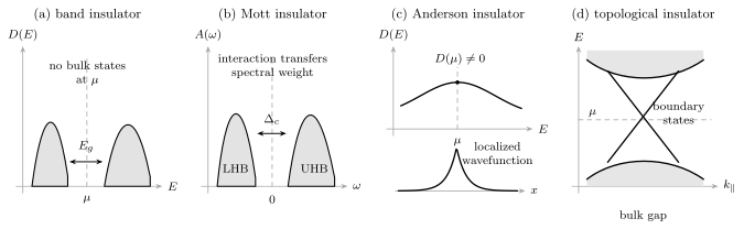
“Insulator” does not identify a unique spectrum or mechanism. A band insulator lacks bulk states at ; a Mott insulator has an interaction-driven charge gap ; an Anderson insulator can have but localized states; a topological insulator has an insulating bulk while symmetry-protected boundary states cross the gap.
Mott Insulators
Section titled “Mott Insulators”A partially filled independent-electron band ordinarily supplies mobile charge, but interactions can instead produce an incompressible state at commensurate filling. This Mott mechanism is distinct from band filling, Anderson localization, and symmetry-induced band reconstruction. Magnetic order commonly coexists with it but is not its definition.
Mott Insulators owns the thermodynamic charge gap, Hubbard and charge-transfer material regimes, bandwidth and filling control, Mott–Slater distinctions, and experimental evidence. The Hubbard Model owns the model construction and controlled limits.
Anderson Insulators
Section titled “Anderson Insulators”Disorder can leave a finite density of one-particle states at the chemical potential while localizing those states, so the zero-temperature dc conductivity vanishes without a hard spectral gap. The obstruction is absence of long-distance diffusion, not absence of available energies. This separates an Anderson insulator from an ideal band insulator and from an interaction-driven Mott insulator.
Anderson Localization owns the random-lattice model, wavefunction and Green-function decay, participation ratios, transfer matrices, dimensional dependence, and zero-temperature localization diagnostics. Anderson Insulators owns the localized-side transport problem: phonon-assisted Miller–Abrahams networks, Mott variable-range hopping, the interaction-induced Coulomb gap, and Efros–Shklovskii hopping.
In three dimensions a Mobility Edge can separate localized and extended states at different energies even while the density of states remains smooth. Finite size, dephasing, interactions, contacts, and hopping all complicate the strict zero-temperature limit, so an insulating temperature dependence alone does not uniquely establish Anderson localization.
Topological Insulators
Section titled “Topological Insulators”A noninteracting topological insulator is a band insulator whose occupied Bloch-state subspace cannot be continuously deformed to an ordinary atomic insulator while preserving the relevant gap and symmetries.
The bulk energy spectrum can look fully gapped in both cases. The distinction resides in the global geometry of the occupied eigenvectors.
For a two-dimensional Chern insulator,
and
A time-reversal-invariant topological insulator instead uses a invariant rather than a nonzero total Chern number. When the protecting symmetry is preserved and the boundary is suitable, gapless or anomalous boundary states accompany the nontrivial bulk.
Boundary conduction does not make the bulk metallic. Conversely, a surface can be disordered, doped, hybridized in a thin film, or gapped by symmetry breaking without erasing every bulk topological distinction.
The Quantum Hall Geometry Preview introduces the geometric response viewpoint. Topological Insulators owns the time-reversal-protected classification, helical edges, surface Dirac cones, and materials ledger; the quantum Hall pages own their corresponding Hall phases.
Quantum Hall Insulators
Section titled “Quantum Hall Insulators”In an integer quantum Hall plateau, the two-dimensional bulk has a spectral or mobility gap for longitudinal transport while
and
Chiral edge states carry boundary current. Calling the state simply “insulating” hides the quantized transverse response; calling it simply “conducting” hides the gapped bulk. The conductivity tensor and geometry must be stated.
Fractional quantum Hall states go further: interactions and topological order produce fractionalized excitations and cannot be reduced to occupied noninteracting electron bands.
Comparing Mechanisms
Section titled “Comparing Mechanisms”| State | Spectral or charge structure | State character near | Zero-temperature bulk longitudinal response |
|---|---|---|---|
| Fermi-liquid metal | gapless Fermi surface | extended quasiparticles | metallic; ideal clean model has Drude weight |
| Band insulator | positive band and charge gap | no bulk states at | insulating |
| Intrinsic semiconductor | positive controllable band gap | thermally activated carriers at | insulating at ideal |
| Overlap semimetal | electron and hole pockets | extended, low density | metallic or semimetallic |
| Nodal semimetal | point or line touching | extended but vanishing phase space possible | gapless; response is dimension and disorder dependent |
| Mott insulator | interaction-driven charge gap | correlated spectral weight away from | insulating |
| Anderson insulator | no necessary spectral gap | localized | insulating |
| Topological band insulator | bulk band gap plus nontrivial occupied subspace | bulk gapped, boundary states possible | bulk insulating; boundary or Hall response can remain |
Experimental Diagnosis
Section titled “Experimental Diagnosis”No single measurement settles the mechanism.
Electrical transport
Section titled “Electrical transport”Measure longitudinal and Hall tensors over temperature, field, orientation, thickness, and carrier tuning. Activated resistivity is evidence for an energy or mobility scale, not by itself a proof of a band gap.
ARPES and tunneling
Section titled “ARPES and tunneling”ARPES measures occupied momentum-resolved spectral weight; tunneling probes local spectral density. They can reveal gaps and coherence, but matrix elements, surfaces, disorder, and finite resolution matter. A transport insulator can retain a finite local density of localized states.
Optical spectroscopy
Section titled “Optical spectroscopy”Optical absorption probes neutral transitions and matrix elements. Excitons, phonon assistance, indirect gaps, and forbidden transitions separate optical thresholds from the fundamental charge gap.
Thermodynamics and compressibility
Section titled “Thermodynamics and compressibility”Electronic heat capacity, magnetic susceptibility, and charge compressibility test low-energy state density and interactions. Neutral excitations can survive in an electrical insulator.
Spatial and boundary probes
Section titled “Spatial and boundary probes”Thickness scaling, nonlocal transport, scanning probes, and boundary-sensitive spectroscopy help distinguish bulk conduction, surface conduction, hopping networks, and edge channels.
Parameter tuning
Section titled “Parameter tuning”Gate voltage, pressure, strain, disorder, and magnetic field can reveal whether a gap closes, a mobility edge moves, symmetry changes, or spectral weight transfers across a correlation scale.
The strongest classification is a consistent account of several observables using one mechanism and one declared limit.
A Practical Decision Tree
Section titled “A Practical Decision Tree”- Specify the limit. State temperature, frequency, sample dimension, thermodynamic limit, and whether bulk or boundary response is meant.
- Check translation and symmetry. Use the correct primitive cell, magnetic order, and disorder description.
- Determine the charge spectrum. Is there a band gap, many-body charge gap, pseudogap, or no gap?
- Determine state character. Are states near extended, localized, coherent, or fractionalized?
- Check filling and Fermi geometry. Identify full bands, pockets, nodes, and degeneracies.
- Compare transport and spectroscopy. A mismatch can diagnose localization, excitons, contacts, or incoherence.
- Test topology and boundaries. Energies alone do not classify occupied-state geometry.
- Vary a control parameter. Distinguish robust mechanism from a fit over one narrow regime.
Common Mistakes
Section titled “Common Mistakes”Equating zero density of states with insulation
Section titled “Equating zero density of states with insulation”A nodal semimetal can be gapless with .
Equating nonzero density of states with metallicity
Section titled “Equating nonzero density of states with metallicity”Localized Anderson states can give without dc diffusion.
Calling every positive-gap crystal a semiconductor
Section titled “Calling every positive-gap crystal a semiconductor”Semiconductor is a practical materials category within band insulators, not a sharply separate zero-temperature phase.
Reading the transport gap as the band gap
Section titled “Reading the transport gap as the band gap”Defects, hopping, mobility edges, contacts, and dopant ionization can set the activation energy.
Calling a half-filled-band insulator automatically Mott
Section titled “Calling a half-filled-band insulator automatically Mott”Symmetry breaking, hybridization, disorder, or a larger actual primitive cell may open the gap.
Calling a magnetic insulator automatically Slater
Section titled “Calling a magnetic insulator automatically Slater”Magnetic order can coexist with a pre-existing interaction-driven Mott gap.
Calling a topological insulator metallic because its surface conducts
Section titled “Calling a topological insulator metallic because its surface conducts”The adjective describes the bulk band topology; boundary and bulk responses must be separated.
Treating zero resistance as ordinary metallicity
Section titled “Treating zero resistance as ordinary metallicity”Superconductivity has condensate stiffness and pairing coherence, not merely absent impurity scattering.
Exercises
Section titled “Exercises”Exercise 1: filling a cosine band
Section titled “Exercise 1: filling a cosine band”A one-dimensional spin-degenerate band has
and is separated from all other bands. Classify the independent-electron ground state at one and two electrons per primitive cell.
Solution
The displayed spin-degenerate band holds two electrons per cell.
At one electron per cell it is half filled. The chemical potential crosses the band, producing two Fermi points in the simple one-dimensional model. Independent-electron band theory predicts a metal.
At two electrons per cell the band is full. Because the problem states that the next band is separated by a positive global gap, the model predicts a band insulator.
In one dimension, interactions can destabilize the half-filled metallic prediction, so the first answer is explicitly an independent-electron classification.
Exercise 2: intrinsic density and chemical potential
Section titled “Exercise 2: intrinsic density and chemical potential”Derive and from the nondegenerate electron and hole densities.
Solution
Set :
Taking logarithms and solving for gives
Multiplying the two densities,
Since and ,
Exercise 3: activation slope
Section titled “Exercise 3: activation slope”An intrinsic semiconductor has temperature-independent mobilities over a restricted range and . What activation energy appears in versus ? Why can an experimental slope differ?
Solution
With fixed mobilities,
Ignoring the algebraic factors in and ,
The ideal Arrhenius slope corresponds to
An observed slope can differ because mobilities vary with temperature, dopant ionization or hopping dominates, contacts add barriers, the chemical potential is not intrinsic, or the gap itself changes with temperature.
Exercise 4: Dirac semimetal state count
Section titled “Exercise 4: Dirac semimetal state count”For a three-dimensional isotropic Dirac cone with degeneracy , derive the carrier density at .
Solution
The Fermi wavevector satisfies
The occupied conduction-band volume is
State counting per physical volume gives
Differentiating with respect to yields
which vanishes at neutrality despite the absence of a gap.
Exercise 5: atomic Mott gap
Section titled “Exercise 5: atomic Mott gap”At , consider one Hubbard site per cell at one electron per site. Show that the charge gap is .
Solution
At one electron per site there is no double occupancy, so choose the reference interaction energy as zero.
Removing one electron creates an empty site and costs no interaction energy:
Adding one electron forces one site to be doubly occupied and costs
Therefore
Finite hopping lowers and broadens the addition and removal thresholds; the gap is no longer exactly .
Exercise 6: inverse participation ratio
Section titled “Exercise 6: inverse participation ratio”Evaluate the scaling of the inverse participation ratio for (a) a state uniform over sites and (b) a state uniform over sites with fixed as .
Solution
For a state uniform over sites,
Hence
For a state uniform over only sites,
If remains fixed, the IPR remains finite in the thermodynamic limit, which is characteristic of localization.
Exercise 7: classify the evidence
Section titled “Exercise 7: classify the evidence”Match each observation to the most direct classification, while stating what remains unproved:
- a full bulk gap, an odd number of robust surface crossings, and insulating thickness-dependent bulk transport;
- finite tunneling density at but exponentially localized wavefunctions and vanishing zero-temperature diffusion;
- an activated intrinsic carrier density obeying ;
- zero resistance below a critical temperature and a phase-stiff condensate.
Solution
- The evidence supports a topological insulator, provided the protecting symmetry and bulk invariant are established. Surface crossings alone can be mimicked by trivial surface states.
- This is an Anderson-insulating mechanism: states exist at but are localized. The evidence does not by itself decide the role of interactions.
- This is intrinsic semiconductor behavior in the stated regime. The slope alone does not prove the microscopic band gap without excluding mobility and defect effects.
- This is a superconductor, not merely an unusually good normal metal. Phase stiffness distinguishes condensate transport from a long normal-state scattering time.
Connections
Section titled “Connections”- Band Theory Overview defines bands, filling, and chemical potential.
- Band Gaps owns the direct, global, charge, quasiparticle, Kohn–Sham, optical, transport, and mobility-gap ledger.
- Fermi Surface develops electron and hole pockets, compensation, and gapless metallic phase space.
- Density of States distinguishes spectral state count from velocity and localization information.
- Hubbard Model is the canonical model home for interaction-driven Mott physics.
- Anderson Localization owns microscopic localization and its eigenstate, transfer-matrix, and conductance diagnostics.
- Anderson Insulators develops gapless insulating response, bath-assisted hopping, Mott optimization, Coulomb gaps, and mechanism-aware transport tests.
- Fermi-Liquid Theory Preview describes the conventional interacting metal.
- Quantum Hall Geometry Preview introduces filled-band geometry and quantized transverse response.
- Effective Mass explains electron and hole curvature, anisotropic band edges, and why transport, cyclotron, optical, and density-of-states masses can differ.
- Drude Theory develops the simplest finite-lifetime metal response and its clean, multiband, Hall, and optical limits.
References
Section titled “References”- N. W. Ashcroft and N. D. Mermin, Solid State Physics (Holt, Rinehart and Winston, 1976), Chapters 1–2, 12–13, and 28.
- C. Kittel, Introduction to Solid State Physics, 8th ed. (Wiley, 2005), Chapters 6–8.
- P. Y. Yu and M. Cardona, Fundamentals of Semiconductors, 4th ed. (Springer, 2010), Chapters 2–4.
- S. M. Sze and K. K. Ng, Physics of Semiconductor Devices, 3rd ed. (Wiley, 2006), Chapters 1–2.
- W. Kohn, “Theory of the Insulating State,” Physical Review 133, A171–A181 (1964), doi:10.1103/PhysRev.133.A171.
- N. F. Mott, Metal-Insulator Transitions, 2nd ed. (Taylor & Francis, 1990).
- P. W. Anderson, “Absence of Diffusion in Certain Random Lattices,” Physical Review 109, 1492–1505 (1958), doi:10.1103/PhysRev.109.1492.
- D. J. Thouless, M. Kohmoto, M. P. Nightingale, and M. den Nijs, “Quantized Hall Conductance in a Two-Dimensional Periodic Potential,” Physical Review Letters 49, 405–408 (1982), doi:10.1103/PhysRevLett.49.405.
- C. L. Kane and E. J. Mele, “ Topological Order and the Quantum Spin Hall Effect,” Physical Review Letters 95, 146802 (2005), doi:10.1103/PhysRevLett.95.146802.
- M. Z. Hasan and C. L. Kane, “Colloquium: Topological insulators,” Reviews of Modern Physics 82, 3045–3067 (2010), doi:10.1103/RevModPhys.82.3045.