Semiconductor Lasers Overview
A semiconductor laser converts nonequilibrium electrons and holes into a coherent optical field. Its gain medium, waveguide, and often much of its resonator are fabricated in one semiconductor structure. The resulting source can be efficient, compact, directly current modulated, and available near many atomic and molecular transitions.
Those advantages come with coupled control variables. Injection current changes carrier density, gain, refractive index, temperature, optical power, and frequency. A milliwatt-scale reflection can be a strong perturbation because it re-enters a microscopic cavity. The bare chip’s gain bandwidth is broad compared with an atomic line, while its longitudinal modes are far closer together than the gain bandwidth. Using a diode laser in AMO physics therefore requires both semiconductor gain physics and careful optical control.
Canonical Scope
Section titled “Canonical Scope”This page owns:
- interband gain in terms of carrier occupations and quasi-Fermi levels;
- the Bernard–Duraffourg condition for positive stimulated gain;
- carrier and optical confinement in heterostructures and quantum wells;
- threshold, longitudinal-mode selection, and output of injection diodes;
- the distinction among Fabry–Pérot, DFB, DBR, VCSEL, and external-cavity devices;
- Littrow and Littman–Metcalf external-cavity diode lasers;
- current, temperature, grating, cavity-length, and electronic tuning;
- carrier-induced amplitude–phase coupling and optical-feedback sensitivity;
- practical source architectures and diagnostics for AMO experiments.
Population Inversion owns the general inversion concept. Gain and Threshold owns the medium-independent round-trip threshold logic. Rate-Equation Lasers owns transient carrier–photon dynamics, relaxation oscillations, and small-signal response. Linewidth and Coherence owns phase-noise definitions and linewidth measurement. Here those ideas are specialized to semiconductor devices without repeating their canonical derivations.
Convention Ledger
Section titled “Convention Ledger”Unless stated otherwise:
- is angular frequency and is ordinary frequency;
- and are electron occupations in conduction- and valence-band states connected by an optical transition;
- the corresponding hole occupation is ;
- and are electron and hole quasi-Fermi levels written in the usual electron-energy band diagram;
- is a material intensity gain coefficient, so an unconfined traveling intensity obeys ;
- is the optical confinement factor, making the modal intensity gain;
- and are distributed internal and mirror intensity losses per unit length;
- and are facet power reflectivities;
- denotes a carrier-pair density when charge neutrality permits one density to represent injected electrons and holes;
- is diode current, is current density, and is the elementary charge;
- is the physical chip-cavity length and its group index;
- is an optical path length, not necessarily a geometric length.
Field-gain coefficients, amplitude reflectivities, angular-frequency linewidths, and alternate signs for the linewidth-enhancement parameter are common in the literature. Converting those conventions before comparing formulas is part of the calculation.
Gain in Semiconductors
Section titled “Gain in Semiconductors”Why bands change the inversion language
Section titled “Why bands change the inversion language”An isolated two-level atom has a discrete upper and lower state. A bulk semiconductor instead has many conduction- and valence-band states. For a direct-gap material, an optical transition approximately conserves crystal momentum: a conduction state and valence state at the same are connected, up to the negligible photon momentum on the Brillouin-zone scale.
For one such pair of states:
- stimulated emission is proportional to ;
- absorption is proportional to .
Their difference is
Positive net stimulated emission at that transition therefore requires . This is the band-state version of inversion. It does not mean that every conduction-band state is more occupied than every valence-band state.
In quasi-equilibrium, rapid intraband scattering lets the two carrier populations be described by separate Fermi–Dirac distributions,
For a vertical transition satisfying
the monotonicity of the Fermi function gives
This is the Bernard–Duraffourg condition. Equality marks transparency for that ideal state pair; a larger quasi-Fermi-level separation makes its stimulated contribution amplifying.
Three distinctions matter:
- is a local spectral gain condition, not the complete laser threshold.
- A measured transparency current is determined by the spectrally and spatially integrated gain, loss, broadening, and confinement, not by one perfectly sharp transition.
- Positive material gain still must exceed cavity loss: .
A microscopic gain schematic
Section titled “A microscopic gain schematic”Within an independent-particle and dipole approximation, the material gain has the schematic form
where is optical polarization, is an interband momentum matrix element, and represents homogeneous and inhomogeneous broadening. The proportionality also contains refractive-index, normalization, and density-of-states factors.
This expression explains why a band gap alone does not determine the laser spectrum. Gain depends on:
- joint density of states;
- dipole matrix elements and polarization selection rules;
- electron and hole distributions;
- temperature and carrier scattering;
- band filling and band-gap renormalization;
- quantum-well subbands and strain;
- many-body Coulomb corrections;
- spatial overlap with the optical mode.
For an indirect-gap semiconductor, momentum conservation normally requires a phonon as well as a photon. That additional process makes ordinary indirect materials such as silicon inefficient interband gain media, although engineered silicon photonics can integrate gain supplied by other materials or other mechanisms.
Double confinement
Section titled “Double confinement”A homojunction can inject carriers, but carriers and photons are poorly confined. A double heterostructure places a lower-band-gap, higher-index active region between higher-band-gap, lower-index claddings:
- band offsets confine injected electrons and holes;
- the refractive-index step guides the optical field;
- recombination is concentrated where the field is largest.
Modern edge emitters usually replace one thick active layer by one or more quantum wells inside a separate-confinement waveguide. Quantum confinement turns the three-dimensional band continuum into subbands and changes the density of states. It can increase differential gain and reduce threshold, but neither result is automatic: carrier leakage, strain, interface quality, well number, optical overlap, and Auger recombination still matter.
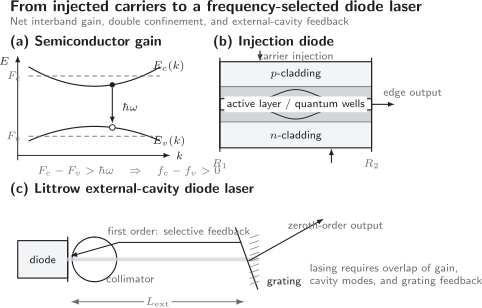
Three connected descriptions of a diode laser. (a) Positive stimulated interband gain requires for the participating states. (b) A double heterostructure or quantum-well waveguide confines both carriers and the optical mode between reflecting facets. (c) A Littrow grating returns a frequency-selective first order while the zeroth order is used as output; lasing occurs where gain, compound-cavity resonances, and grating feedback overlap.
Injection and recombination
Section titled “Injection and recombination”For an active thickness , current density injects carrier pairs at the volume rate
where is an internal injection efficiency. A common phenomenological recombination model is
The terms are conventionally associated with defect-assisted, radiative-bimolecular, and Auger processes. Their coefficients are device, temperature, and density dependent; the form is a useful fit, not a microscopic identity.
Below threshold, increasing current mostly raises carrier density and spontaneous emission. Near transparency, net modal gain approaches zero. Above threshold, stimulated emission strongly clamps the carrier density near its threshold value in an ideal single-mode model, while additional current primarily increases photon number. Leakage, self-heating, gain compression, spatial hole burning, and multimode operation soften that picture.
The coupled carrier and photon equations, including spontaneous-emission coupling and relaxation oscillations, are developed in Rate-Equation Lasers.
Diode Lasers
Section titled “Diode Lasers”Facets make a resonator
Section titled “Facets make a resonator”An edge-emitting chip is a waveguide terminated by two partially reflecting facets. For a round trip of physical length , the intracavity intensity multiplier is
At threshold this multiplier is unity. Therefore
with mirror loss
The lasing frequency must also satisfy a round-trip phase condition. Adjacent longitudinal resonances are separated approximately by
A chip with has . That spacing is large by atomic spectroscopy standards but usually small compared with the semiconductor gain bandwidth. Several chip modes can therefore compete under the same gain envelope.
Facet reflectivity affects more than output power. A lower output-facet reflectivity raises mirror loss and threshold but increases output coupling. An antireflection coating suppresses the internal cavity so an external frequency-selective cavity can dominate. A high-reflection rear facet can direct more useful power toward the output. Coating values must be interpreted with the actual compound-cavity design.
Output above threshold
Section titled “Output above threshold”In an ideal linear approximation above threshold,
where is the external differential quantum efficiency. The slope efficiency is therefore
This relation is a local operating approximation. At high current, self-heating, carrier leakage, gain compression, series resistance, facet heating, and catastrophic optical damage can reduce or terminate the linear regime. A measured light–current curve should report heat-sink temperature and whether the device is operated continuous-wave or pulsed.
Device families
Section titled “Device families”| Device | Frequency selection | Emission geometry | AMO-facing strengths and limits |
|---|---|---|---|
| Fabry–Pérot edge emitter | cleaved-facet longitudinal modes under a broad gain envelope | from chip edge | inexpensive and powerful, but often multimode or mode-hop prone without added selection |
| DFB laser | distributed Bragg grating overlaps the gain region | usually edge emitting | compact single-frequency source with no free-space cavity; tuning range and linewidth depend on design |
| DBR laser | Bragg reflector is separated from at least part of the gain section | usually edge emitting | gain and reflector sections may be tuned separately; integrated devices can offer wide controlled tuning |
| VCSEL | short vertical cavity between semiconductor Bragg mirrors | normal to wafer surface | wafer-scale arrays, low threshold, often circular beam; power, polarization, and wavelength availability vary |
| ECDL | diode plus an external frequency-selective reflector | normally edge-emitter seed | broad tuning, narrower line, and convenient access to alkali wavelengths; mechanically and feedback sensitive |
| Tapered amplifier | seeded traveling-wave semiconductor amplifier | edge output | high power from a narrow-line master, but not a standalone oscillator; adds ASE and spatial-mode concerns |
“Single-mode” can refer to one longitudinal mode, one transverse mode, or one polarization. Those claims are not interchangeable. A device may have a single-frequency core while carrying amplified-spontaneous-emission wings, weak side modes, or polarization switching.
Spatial and polarization properties
Section titled “Spatial and polarization properties”The emitting aperture is strongly asymmetric. Edge emitters generally have:
- a rapidly diverging fast axis and a more slowly diverging slow axis;
- an elliptical, often astigmatic beam;
- polarization favored by the quantum-well and waveguide selection rules;
- residual higher-order spatial structure at high current;
- a wavelength and pointing response to temperature and packaging stress.
A circular-looking beam after one lens is not proof of a diffraction-limited mode. AMO systems commonly use an aspheric collimator, cylindrical correction or anamorphic prisms, and a single-mode or polarization-maintaining fiber. Fiber coupling spatially filters the beam but converts pointing and mode changes into transmitted-power noise.
External-Cavity Diode Lasers
Section titled “External-Cavity Diode Lasers”A compound resonator
Section titled “A compound resonator”An external-cavity diode laser places a frequency-selective reflector outside the chip. The external path does not simply replace the diode cavity unless the output facet is sufficiently antireflection coated. In general the laser is a compound cavity involving:
- the semiconductor gain envelope;
- residual internal-chip resonances;
- external-cavity resonances;
- the wavelength-selective feedback response;
- polarization-dependent losses.
The oscillating mode is the one whose combined round-trip complex gain reaches unity first. Looking only at the grating equation misses internal and external phase conditions; looking only at cavity FSRs misses the gain and feedback envelopes.
Define the one-way group-delay length from the effective rear reflector to the external reflector by
The sum includes the semiconductor chip as well as free-space or other external sections. The corresponding compound-cavity resonance spacing is
A free-space section by itself contributes an FSR scale near , far smaller than a typical chip FSR. The chip’s group delay reduces the actual compound-cavity spacing further. Lengthening the cavity increases photon lifetime and reduces mode spacing, but also adds mechanical sensitivity and more closely spaced modes.
Littrow geometry
Section titled “Littrow geometry”In a conventional Littrow ECDL, a diffraction grating is oriented so the first order retraces the incident beam into the diode. For groove spacing , diffraction order , and Littrow angle ,
The zeroth order supplies the useful output. Rotating the grating changes the selected wavelength, but it also changes the output direction. Many mounts use a compensating mirror or a kinematic arrangement that reduces beam walk.
The grating is simultaneously:
- a dispersive frequency selector;
- an external-cavity end reflector;
- a mechanical element that sets cavity length;
- an output coupler through its zeroth order.
Its efficiency, polarization, illuminated groove number, wavefront quality, and feedback fraction all affect performance. The passive grating resolving power alone does not equal the laser linewidth.
Littman–Metcalf geometry
Section titled “Littman–Metcalf geometry”In a Littman–Metcalf cavity, the grating disperses the diode beam to a tuning mirror, which reflects one selected wavelength back through the grating. The output is commonly taken from the grating zeroth order and remains nearly fixed while the tuning mirror rotates.
| Geometry | Feedback path | Output behavior | Typical tradeoff |
|---|---|---|---|
| Littrow | first diffraction order returns directly to diode | output angle changes with grating rotation unless compensated | simple, efficient, high output |
| Littman–Metcalf | grating plus tuning mirror; light encounters grating twice | nearly fixed output direction | greater selectivity and convenient pointing, but more loss and complexity |
Neither geometry is intrinsically “more stable” in every build. Mechanical lever arms, pivot placement, diode coating, cavity length, grating efficiency, thermal design, and servo implementation often dominate.
Mode-hop-free tuning
Section titled “Mode-hop-free tuning”Tuning the grating envelope while leaving cavity resonances fixed causes the laser to follow one mode only until another mode has lower threshold. The frequency then jumps: a mode hop.
For a selected longitudinal order ,
so continuous tuning along that branch requires
At the same time, grating rotation must move its feedback maximum by the same . A well-chosen mechanical pivot couples grating angle and cavity length approximately correctly. In practice one often co-tunes:
- grating angle or tuning-mirror angle;
- external-cavity length with a piezoelectric actuator;
- diode current to shift index and residual chip modes;
- diode temperature for coarse gain and mode alignment.
“Mode-hop-free over GHz” is an operating claim with specified scan speed, current, temperature, output power, and acceptable side-mode suppression. It is not a permanent property of a mount independent of conditions.
Antireflection-coated and ordinary chips
Section titled “Antireflection-coated and ordinary chips”An antireflection-coated output facet weakens the internal Fabry–Pérot cavity, letting the external grating and cavity dominate. This generally improves continuous tuning and suppresses compound-cavity mode competition, but the chip may not lase safely or usefully without external feedback.
An ordinary commercial diode can also form an ECDL. It is convenient and often inexpensive, yet residual chip modes remain strong. Good operation then requires alignment among chip modes, external modes, and grating feedback. Mode-hop-free scans are typically shorter and more sensitive to current and temperature.
Tuning and Stabilization
Section titled “Tuning and Stabilization”Control inputs are coupled
Section titled “Control inputs are coupled”No actuator changes only one variable.
| Actuator | Principal effects | Typical role | Important limitation |
|---|---|---|---|
| diode current | carrier density, gain, refractive index, junction temperature | fast frequency and power correction; mode alignment | amplitude–frequency coupling, relaxation response, thermal tail |
| diode temperature | band gap, gain peak, refractive index, package length | coarse wavelength selection and slow drift control | slow, hysteretic, large thermal cross-coupling |
| grating or mirror piezo | external-cavity length and often selector angle | medium-bandwidth frequency correction and scans | mechanical resonances, creep, hysteresis, finite travel |
| mechanical grating angle | feedback wavelength and cavity geometry | broad coarse tuning | beam pointing and mode hops |
| AOM | diffracted-beam frequency and amplitude | fast external frequency offset, switching, and intensity control | finite bandwidth and diffraction-efficiency coupling |
| EOM | optical phase, sidebands, or polarization | high-bandwidth phase control and lock modulation | residual amplitude modulation and limited direct frequency range |
The sign and magnitude of a diode’s current-frequency response can change with Fourier frequency. Fast carrier-induced index response and slower thermal response may oppose one another. A servo designed from a DC tuning coefficient alone can therefore become unstable.
Amplitude–phase coupling
Section titled “Amplitude–phase coupling”Changing carrier density changes both material gain and refractive index. In one common convention, with an intensity gain coefficient and ,
The linewidth-enhancement parameter quantifies carrier-induced amplitude–phase coupling near the operating point. Alternate definitions can reverse its sign or absorb factors associated with field rather than intensity gain.
Two consequences are central:
- spontaneous or technical carrier fluctuations convert into phase noise, producing the familiar intrinsic linewidth factor under a restricted single-mode model;
- direct current modulation produces frequency chirp as well as power modulation.
The complete linewidth conventions and their limits are treated in Linewidth and Coherence.
Optical feedback
Section titled “Optical feedback”Light reflected from a window, fiber face, cell, detector, or downstream optic can return after a delay and interfere with the intracavity field. Depending on feedback strength and phase, it can:
- pull or split the frequency;
- narrow or broaden the line;
- create external-cavity side modes;
- cause multistability and hysteresis;
- increase intensity noise;
- drive low-frequency fluctuations or coherence collapse.
A grating-stabilized ECDL deliberately uses controlled feedback; accidental feedback adds another uncontrolled cavity. A Faraday isolator immediately after the source is therefore standard in demanding AMO systems. Isolation must be adequate over wavelength, polarization, and angle, and downstream reflections should still be minimized. Rotating one optic until a noise trace looks quiet is not a substitute for a feedback budget.
What stabilization actually controls
Section titled “What stabilization actually controls”A free-running diode can be tuned near a transition without being stable relative to it. Frequency stabilization requires:
- a reference, such as an atomic discriminator, molecular line, optical cavity, transfer cavity, or another laser;
- an error signal with a declared zero crossing and capture range;
- actuators whose combined response covers the required bandwidth and range;
- loop filtering with measured plant phase and gain;
- an out-of-loop diagnostic whenever accuracy or long-term stability matters.
Atomic references tie the source to a transition but inherit pressure, power, magnetic, line-shape, and modulation shifts. Reference cavities can provide low short-term noise but drift thermally and mechanically. A high-performance system often uses a fast cavity or optical-phase loop plus a slower atomic or absolute reference.
An in-loop error signal can be small while the delivered light is wrong because of detector offsets, residual amplitude modulation, path noise, mode hops, or actuator saturation. Precision Spectroscopy develops reference shifts and uncertainty budgets. Laser Stabilization derives discriminator calibration, closed-loop noise transfer, loop shaping, and out-of-loop validation.
Injection locking and power scaling
Section titled “Injection locking and power scaling”A narrow-line master can seed another diode:
- injection locking forces a slave oscillator to follow the master’s frequency and phase within a locking range;
- a tapered amplifier amplifies a seed without intentionally crossing an oscillator threshold;
- a master-oscillator power-amplifier chain combines spectral control with higher output.
The seed ratio, detuning, polarization, spatial overlap, and back isolation must be controlled. Loss of seed can make a slave or amplifier emit broadband or at an unintended mode. Spectral filtering and interlocks are important when unwanted resonant light would disturb atoms.
Use in AMO Experiments
Section titled “Use in AMO Experiments”Why diode lasers are so common
Section titled “Why diode lasers are so common”Many neutral-atom and ion transitions lie in spectral regions served by III–V semiconductor alloys. Diode systems can supply several independently controlled frequencies without the footprint or electrical power of a large solid-state or dye laser. They are particularly effective when an experiment needs:
- tens of milliwatts to a few watts after amplification;
- narrowband continuous-wave light;
- fast current, AOM, or EOM control;
- several offset frequencies derived from one master;
- robust fiber delivery;
- economical replication across cooling, repumping, detection, and control channels.
Wavelength availability, reliable power, and long-term mode behavior depend on the device generation and package. A data-sheet center wavelength is not a guarantee of single-frequency tuning to a chosen transition over the required temperature and lifetime.
Requirement depends on the experiment
Section titled “Requirement depends on the experiment”| AMO task | Spectral requirement | Additional requirement |
|---|---|---|
| Doppler cooling and fluorescence detection | detuning stable relative to a natural linewidth; controlled side modes | power and polarization stability, switching, low resonant background |
| repumping | correct offset and enough spectral purity to avoid dark-state leakage | reliable simultaneous operation with the cooling source |
| coherent Rabi or Raman control | phase noise integrated over the pulse sequence must be small | deterministic phase, calibrated pulse area, low differential path noise |
| electromagnetically induced transparency | stable one- and two-photon detunings | mutual coherence and controlled control/probe power |
| Ramsey spectroscopy or clocks | low phase noise over free-evolution time and traceable frequency | path-noise control, reference shifts, out-of-loop validation |
| molecular spectroscopy | broad access or agile tuning with known absolute frequency | mode-hop detection, calibrated scans, control of etalons and baselines |
The relevant metric is rarely “laser linewidth” alone. For a Rabi experiment, the weighted phase-noise spectrum over the pulse duration matters. For Raman transitions, relative phase noise between the two optical fields matters more than common optical noise. For cooling, low-frequency drift and intensity or polarization changes may dominate. See Rabi Oscillations, Electromagnetically Induced Transparency, and Ramsey Interferometry for the atomic response.
A practical source chain
Section titled “A practical source chain”A common narrow-line architecture is:
- an ECDL or integrated single-frequency diode as master;
- an optical isolator;
- a pickoff to a reference spectroscopy or cavity lock;
- AOMs or EOMs for offsets, switching, and fast control;
- an injection-locked slave or tapered amplifier when more power is needed;
- spatial filtering and polarization preparation;
- fiber delivery or a stabilized free-space path;
- diagnostics sampled near the experiment.
The order is not universal. Placing an AOM before a fiber may convert AOM pointing into fiber-coupled power noise; placing it after the fiber moves thermal load and alignment near the apparatus. A high-power amplifier before an isolator can demand an expensive isolator and can send damaging return light into the amplifier. Architecture follows the actual power, bandwidth, frequency, and feedback budget.
Diagnose the light at the atoms
Section titled “Diagnose the light at the atoms”Characterizing only the laser head misses downstream changes. Useful measurements include:
- optical power and relative-intensity noise at the delivered port;
- polarization after the final fiber, viewport, or beam splitter;
- beat-note or frequency-noise measurements against an independent source;
- scanning-cavity traces for side modes and mode hops;
- optical spectra for amplified spontaneous emission;
- beam quality, pointing, and fiber-coupling stability;
- an atomic discriminator observed out of loop;
- event logging for current, temperature, piezo voltage, lock state, and amplifier seed.
A wavemeter can identify the coarse mode and detect large hops. It does not by itself establish sub-megahertz linewidth, phase coherence, or accuracy. A scanning Fabry–Pérot can reveal mode structure but must have adequate FSR, finesse, scan linearity, and resolution. An atomic signal is a powerful diagnostic only after optical pumping, power broadening, magnetic fields, and line pulling are understood.
Operational hazards
Section titled “Operational hazards”Laser diodes are sensitive to electrostatic discharge, current overshoot, reverse voltage, overheating, and optical feedback. Good practice includes:
- a low-noise current source with a hard current limit and slow start;
- temperature control with a correctly placed sensor;
- interlocks that turn off current if temperature control fails;
- electrostatic precautions during handling;
- protection against cable disconnect transients;
- gradual power-up of seeded amplifiers;
- eye-safe alignment procedures appropriate to visible and invisible beams.
The emitted wavelength may be invisible while still focused tightly enough to damage an eye. Optical safety is a hardware and procedural requirement, not a final note added after alignment.
Worked Example: Threshold and Mode Scales
Section titled “Worked Example: Threshold and Mode Scales”Consider a edge-emitting diode with , , internal intensity loss , confinement factor , and group index .
The mirror loss is
The required material gain is therefore
The chip FSR is
The calculation separates two questions. The gain condition says how much material amplification is needed. The FSR says where longitudinal resonances can occur. Lasing requires both, together with the spectral gain curve and transverse-mode losses.
Common Mistakes
Section titled “Common Mistakes”- Equating band-gap energy with laser frequency. Band filling, renormalization, quantum-well subbands, temperature, cavity modes, and frequency-selective feedback all shift the oscillation frequency.
- Calling any injected carrier population an inversion. Net stimulated gain at requires , equivalently under the stated quasi-equilibrium assumptions.
- Confusing positive gain with threshold. Threshold additionally requires modal gain to equal internal and output-coupling loss.
- Mixing field and intensity coefficients. Field amplitudes and intensities acquire factors of two in propagation and decay exponents.
- Using phase index in the FSR without thought. Longitudinal-mode spacing is governed by group delay and therefore in a dispersive cavity.
- Treating an ECDL as one empty external cavity. Residual chip modes, carrier-induced phase, grating feedback, and the gain envelope form a compound resonator.
- Scanning only the grating. Continuous tuning requires selector and cavity resonances to move together, often with current co-tuning.
- Interpreting a quiet in-loop signal as proof of delivered stability. Offsets, path noise, mode hops, and actuator saturation can remain hidden.
- Ignoring back reflections. A weak returned field can reorganize a semiconductor laser’s spectrum and dynamics.
- Checking spectrum but not phase or vice versa. Side-mode suppression, linewidth, integrated phase noise, drift, and absolute accuracy answer different experimental questions.
- Assuming fiber delivery fixes the beam. It filters spatial mode but can translate pointing, polarization, and frequency-dependent coupling into delivered power fluctuations.
- Quoting performance without conditions. Current, heat-sink temperature, scan rate, measurement bandwidth, reference, and optical feedback environment belong with the number.
Exercises
Section titled “Exercises”1. Stimulated-emission balance
Section titled “1. Stimulated-emission balance”At one vertical transition, let and . Calculate the occupation factors for stimulated emission and absorption, and find their difference.
Solution
The stimulated-emission factor is
The absorption factor is
Their difference is
The state pair contributes positive net stimulated gain. This does not yet establish modal threshold.
2. Quasi-Fermi-level condition
Section titled “2. Quasi-Fermi-level condition”A transition has photon energy . Evaluate whether it is absorbing, transparent, or amplifying in the ideal state-pair sense when is (a) , (b) , and (c) .
Solution
The Bernard–Duraffourg comparison is
Therefore:
- (a) : net absorption;
- (b) : state-pair transparency;
- (c) : positive stimulated gain.
Real material transparency is spectrally broadened and integrated over many states, so one equality should not be overinterpreted as a measured device current.
3. Modal threshold
Section titled “3. Modal threshold”A diode has , , , , and . Find the mirror loss and threshold material gain.
Solution
Convert the length:
Then
Thus
This uses power reflectivities and intensity gain and loss coefficients.
4. Chip and external-cavity mode scales
Section titled “4. Chip and external-cavity mode scales”A chip has . It is used in an ECDL with a one-way free-space section between its output facet and grating. Estimate the isolated chip FSR and the compound-cavity FSR, treating the rear facet as the other effective reflector.
Solution
For the chip,
The compound-cavity group-delay length is
Therefore
The external modes are much more closely spaced. With an uncoated diode, lasing still depends on both mode families rather than the external FSR alone.
5. Differential efficiency
Section titled “5. Differential efficiency”A diode has external differential quantum efficiency . Estimate its ideal slope efficiency in .
Solution
Use
Numerically,
This is a local ideal slope. Thermal rollover and internal loss can reduce the measured value.
6. Co-tuning an external cavity
Section titled “6. Co-tuning an external cavity”An ECDL has external optical path and operates at . What optical-path change keeps the same external longitudinal order while the laser frequency increases by ?
Solution
At fixed longitudinal order,
Therefore
The optical path must shorten. The grating feedback maximum and residual chip mode must also move consistently; changing length alone does not guarantee a mode-hop-free scan.
7. Linewidth-enhancement parameter
Section titled “7. Linewidth-enhancement parameter”At one operating point and under the page’s intensity-gain convention, let , , and . Estimate .
Solution
Use
Then
The sign follows the declared convention. A source using field gain or the opposite susceptibility sign may quote a different algebraic definition while predicting the same measurable coupling.
8. Design an AMO source diagnostic
Section titled “8. Design an AMO source diagnostic”A Raman experiment derives two optical frequencies from one ECDL. The single-laser beat against an independent reference is narrow, but Raman contrast decays rapidly as the pulse separation grows. Name at least four diagnostics or design checks that distinguish laser noise from differential delivery-path noise.
Solution
A useful investigation includes:
- beat the two Raman fields against each other after their separate AOM, fiber, and free-space paths, preferably near the atoms;
- compare that out-of-loop relative-phase noise with the master laser’s independent optical beat;
- vary path length, fiber routing, acoustic shielding, and common-path fraction to test differential sensitivity;
- log AOM radio-frequency phase and reference-clock coherence;
- measure fiber-coupling power and polarization to identify pointing-to-phase or polarization effects;
- repeat with both tones propagated through a common modulator and fiber;
- search for cycle slips, mode hops, and actuator saturation synchronized with lost contrast;
- compute the Raman sequence’s phase-noise sensitivity function rather than comparing only quoted optical FWHMs.
Common master-laser phase noise can cancel strongly in a Raman difference. A narrow independent optical beat therefore does not rule out differential path or radio-frequency phase noise.
References
Section titled “References”- M. G. A. Bernard and G. Duraffourg, “Laser Conditions in Semiconductors”, physica status solidi (b) 1, 699–703 (1961). Quasi-Fermi-level condition for positive semiconductor gain.
- R. N. Hall, G. E. Fenner, J. D. Kingsley, T. J. Soltys, and R. O. Carlson, “Coherent Light Emission From GaAs Junctions”, Physical Review Letters 9, 366–368 (1962). Early GaAs injection-laser demonstration.
- I. Hayashi, M. B. Panish, P. W. Foy, and S. Sumski, “Junction Lasers Which Operate Continuously at Room Temperature”, Applied Physics Letters 17, 109–111 (1970). Continuous-wave double-heterostructure operation at room temperature.
- H. Kogelnik and C. V. Shank, “Coupled-Wave Theory of Distributed Feedback Lasers”, Journal of Applied Physics 43, 2327–2335 (1972). Canonical DFB coupled-mode theory.
- H. Soda, K. Iga, C. Kitahara, and Y. Suematsu, “GaInAsP/InP Surface Emitting Injection Lasers”, Japanese Journal of Applied Physics 18, 2329–2330 (1979). Early vertical-cavity surface-emitting laser.
- R. Lang and K. Kobayashi, “External Optical Feedback Effects on Semiconductor Injection Laser Properties”, IEEE Journal of Quantum Electronics 16, 347–355 (1980). Compound-cavity and delayed optical-feedback effects.
- C. H. Henry, “Theory of the Linewidth of Semiconductor Lasers”, IEEE Journal of Quantum Electronics 18, 259–264 (1982). Carrier-induced amplitude–phase coupling and linewidth enhancement.
- C. E. Wieman and L. Hollberg, “Using Diode Lasers for Atomic Physics”, Review of Scientific Instruments 62, 1–20 (1991). Foundational AMO-oriented review of diode-laser control and applications.
- L. Ricci, M. Weidemüller, T. Esslinger, A. Hemmerich, C. Zimmermann, V. Vuletić, W. König, and T. W. Hänsch, “A Compact Grating-Stabilized Diode Laser System for Atomic Physics”, Optics Communications 117, 541–549 (1995).
- A. S. Arnold, J. S. Wilson, and M. G. Boshier, “A Simple Extended-Cavity Diode Laser”, Review of Scientific Instruments 69, 1236–1239 (1998).
- C. J. Hawthorn, K. P. Weber, and R. E. Scholten, “Littrow Configuration Tunable External Cavity Diode Laser with Fixed Direction Output Beam”, Review of Scientific Instruments 72, 4477–4479 (2001).
- L. A. Coldren, S. W. Corzine, and M. L. Mašanović, Diode Lasers and Photonic Integrated Circuits, 2nd ed., Wiley (2012). Device physics, gain, resonators, modulation, and integrated architectures.
- G. P. Agrawal and N. K. Dutta, Semiconductor Lasers, 2nd ed., Van Nostrand Reinhold (1993). Graduate treatment of semiconductor gain, dynamics, noise, and device structures.
- A. E. Siegman, Lasers, University Science Books (1986). General laser resonators, gain, mode selection, and linewidth conventions.
- Royal Swedish Academy of Sciences, “The Nobel Prize in Physics 2000: Advanced Information” (2000). Historical and physical account of semiconductor heterostructures and double-confinement lasers.
- National Institute of Standards and Technology, “Diode Laser Technology”, accessed 25 July 2026. NIST overview and bibliography for diode-laser development and metrology.
Further Connections
Section titled “Further Connections”- Quantum Wells develops the confinement energies, envelope overlap, two-dimensional joint state counting, and selection rules behind quantum-well gain media.
- Lasers Overview
- Population Inversion
- Gain and Threshold
- Rate-Equation Lasers
- Optical Cavities
- Laser Modes
- Linewidth and Coherence
- Precision Spectroscopy
- Line Shapes and Broadening
- Rabi Oscillations
- Electromagnetically Induced Transparency
- Ramsey Interferometry