Quantum Wells
A quantum well confines a carrier strongly in one spatial direction while leaving it extended in the other two. The confined coordinate produces discrete levels; each level becomes a two-dimensional subband because the in-plane wavevector remains continuous. This spectral definition matters more than the visual thinness of a layer.
A thin film is not automatically in the quantum-well regime. Its confinement spacing must be resolved against temperature, disorder, lifetime broadening, and any energy window explored by the measurement. Conversely, a carrier can occupy a quantum well defined by band bending or electrostatic gates even when there is no sharply bounded material layer.
This page is the canonical home for one-direction confinement, envelope-function matching at heterointerfaces, quantum-well subbands and density of states, band alignment, interband and intersubband optical selection rules, and the distinction between a well and an occupied two-dimensional electron or hole system. Finite Square Well owns the exact transcendental equations for the elementary one-dimensional potential. Effective Mass owns the band-curvature approximation. Coupled Wells and Avoided Crossings owns the two-state tunneling reduction. Two-Dimensional Electron Gases owns mobility, disorder, collective response, quantum Hall use, and oxide-interface physics once the layer is populated.
Operational Definition
Section titled “Operational Definition”Let the confining direction be , and let denote position in the layer. A useful single-subband quantum-well hierarchy is
where is the first confinement spacing, is static or lifetime broadening, and is any finite observation time that limits energy resolution. The stronger condition
at zero temperature places the chemical potential below the second subband threshold. These are separate statements:
- resolved confinement means individual subbands can be distinguished;
- single-subband occupation means only the lowest threshold is populated;
- phase coherence concerns interference and need not extend across the sample merely because confinement is quantized;
- two-dimensional kinematics means the active low-energy motion is in the plane;
- a two-dimensional electron gas additionally requires an occupied carrier population.
The well width alone therefore does not classify the system. Effective mass, barrier height, carrier density, temperature, disorder, and probe frequency all enter.
Envelope-Function Hamiltonian
Section titled “Envelope-Function Hamiltonian”Near a nondegenerate band extremum, a slowly varying heterostructure can often be modeled by a one-band envelope Hamiltonian
Here is the relevant conduction- or valence-band edge including applied electrostatic potentials, and is the effective mass along the growth direction. The confined envelopes solve
For a translationally invariant layer with constant in-plane masses, the full state factorizes as
and its dispersion is
The rapidly varying Bloch factor carries the microscopic orbital and spin structure. The envelope describes variation over many lattice spacings. This separation is controlled only when the structure varies slowly enough on the atomic scale and the retained band is sufficiently isolated.
Interface matching and current conservation
Section titled “Interface matching and current conservation”For the displayed position-dependent-mass operator, integrating the Schrödinger equation across an abrupt interface without a singular potential gives the BenDaniel–Duke matching conditions
The second condition is not arbitrary. It makes the normal probability current
continuous across the interface. Requiring the ordinary derivative to be continuous when the mass changes generally violates this current ledger.
These conditions belong to a particular one-band effective Hamiltonian. Atomically abrupt interfaces, strongly coupled conduction and valence bands, heavy- and light-hole mixing, nonparabolicity, intervalley coupling, and interface-specific terms may require a multiband or microscopic model. There is no universal license to insert a discontinuous effective mass into any operator ordering and retain the same boundary conditions.
Infinite-Well Benchmark
Section titled “Infinite-Well Benchmark”For an ideal well of width with impenetrable barriers,
The scaling is the most transferable lesson. For a GaAs well with , this benchmark gives
and hence . A finite barrier lowers these energies relative to the same-width infinite well and allows wavefunction penetration into the barrier. Material-dependent masses, band offsets, strain, and electrostatic fields further change the result. The benchmark is a scale estimate, not a prediction for a specified heterostructure.
For a finite well, the number of bound levels is finite. The rigorous transcendental solution is developed at Finite Square Well; in a heterostructure, one must also use the appropriate masses and interface conditions.
From Bound Levels to Subbands
Section titled “From Bound Levels to Subbands”Every confined eigenvalue is a threshold for in-plane motion. In an isotropic parabolic band,
States in one subband share the same -profile but have different in-plane wavelengths. Occupying more in-plane momentum does not excite the transverse coordinate until the total energy reaches another threshold.
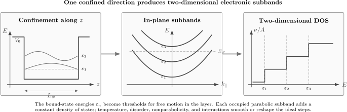
One-direction confinement produces discrete energies , while free motion in the layer turns each energy into a two-dimensional subband. For ideal parabolic subbands, each threshold adds a constant contribution to the density of states per unit area.
The dimensional distinction from neighboring structures is now precise:
| Structure | Confined directions | Extended directions | Ideal low-energy spectrum |
|---|---|---|---|
| bulk crystal | 0 | 3 | three-dimensional bands |
| quantum well | 1 | 2 | two-dimensional subbands |
| quantum wire | 2 | 1 | one-dimensional subbands |
| quantum dot | 3 | 0 | discrete orbitals |
Quantum Wires develops the one-dimensional threshold singularity and mode counting. Quantum Dots develops the fully discrete spectrum together with charging and reservoir coupling.
Two-Dimensional Density of States
Section titled “Two-Dimensional Density of States”For a sample area with periodic boundary conditions, one state per internal component occupies area in the plane. The number of states in subband below energy is therefore
where includes unresolved spin, valley, or other degeneracies. For an isotropic parabolic subband,
Differentiation gives the ideal density of states per unit area:
Each subband contributes a constant step. With spin degeneracy , a single isotropic subband contributes . For elliptical contours,
so the density-of-states mass is . This need not equal a transport or cyclotron mass; Effective Mass keeps those definitions separate.
At zero temperature, the sheet density is
At finite temperature,
The ideal steps are rounded by temperature and lifetime broadening. Disorder can create tails or localized states, interactions can modify the compressibility and spectral function, and nonparabolicity makes the step height energy dependent. A measured shoulder is evidence for a subband threshold only after these alternatives and the probe response have been modeled.
Heterostructure Confinement
Section titled “Heterostructure Confinement”Most semiconductor quantum wells are heterostructures: a narrower-gap layer is placed between materials whose band edges form barriers. The relevant potential is not the band gap alone. One needs the conduction- and valence-band offsets, strain shifts, electrostatic band bending, polarization fields, interface dipoles, and alloy composition.
Band-alignment types
Section titled “Band-alignment types”| Alignment | Band-edge relation | Typical carrier arrangement | Optical consequence |
|---|---|---|---|
| type I, straddling | electron and hole wells lie in the same material | both carrier species localized in one layer | strong spatial overlap is possible |
| type II, staggered | electron and hole minima favor different layers | carriers spatially separated | lower overlap, long-lived indirect excitons possible |
| type III, broken gap | one material’s conduction edge lies below the other’s valence edge | electron- and hole-like states can overlap energetically | hybridization and charge transfer become central |
Band-offset ratios quoted for one alloy composition, strain state, temperature, or interface should not be exported uncritically to another. For quantitative work, material parameters and their conventions must be documented, and uncertainty in the offsets should be propagated to predicted levels.
Coupled wells and superlattices
Section titled “Coupled wells and superlattices”Two nearby wells hybridize through their barrier. If and are localized lowest-well states, a useful reduction is
At resonance, tunneling produces symmetric and antisymmetric states split by . Detuning produces an avoided crossing rather than a true crossing; the canonical derivation is at Coupled Wells and Avoided Crossings.
Repeating wells periodically creates a superlattice. The discrete level of one isolated well broadens into a miniband whose width depends exponentially on barrier thickness in the weak-coupling limit. Finite stacks, disorder, internal electric fields, and contacts break the ideal translational symmetry. Resonant Transmission owns the scattering formulation for a level between barriers.
Self-consistent electrostatics
Section titled “Self-consistent electrostatics”In a populated or doped structure, the carrier density changes the confining potential. A minimal calculation iterates the envelope equation with Poisson’s equation,
The charge density includes mobile carriers, ionized dopants, gates, fixed interface charge, and polarization charge. denotes an optional exchange-correlation approximation, not an exact correction. Boundary conditions and global charge neutrality matter as much as the differential equation. Solving a fixed square well and then inserting an arbitrarily large sheet density is not self-consistent.
Optical Transitions
Section titled “Optical Transitions”Quantum wells are powerful optical platforms because confinement changes transition energies, oscillator strengths, polarization selection rules, and the joint density of states. Three distinct ledgers should not be conflated: interband transitions create or annihilate an electron–hole pair, intersubband transitions move a carrier between envelopes in the same band, and excitonic resonances include electron–hole attraction.
Interband transitions and excitons
Section titled “Interband transitions and excitons”In a simple independent-particle picture, an electron subband and a hole subband give a transition near
An excitonic resonance is lower by a binding energy:
This is an organizing equation, not a universal fit formula. Strain, band mixing, dielectric confinement, Coulomb correlations, band-gap renormalization, exchange, disorder, and carrier screening can all matter.
For a slowly varying optical field, the envelope contribution to the interband matrix element contains
In an ideal symmetric well with similar electron and hole boundary conditions, orthogonality makes transitions strongest in the simplest model. The complete rule also includes the zone-center Bloch matrix element, light polarization, heavy- and light-hole mixing, strain, and symmetry breaking. “Only equal subband indices are allowed” is therefore an approximation with stated assumptions, not an exact material-independent law.
The two-dimensional joint density of states produces step-like continua in an independent-particle model, while Coulomb attraction transfers oscillator strength into excitonic resonances. Absorption and photoluminescence are not interchangeable: absorption probes allowed initial-to-final transitions, whereas luminescence also depends on nonequilibrium populations, relaxation, and nonradiative loss.
Intersubband transitions
Section titled “Intersubband transitions”An electron already in one conduction subband can absorb a photon and move to another. In the electric-dipole approximation the relevant envelope matrix element is
The optical electric field must have a component along the growth direction. An ideal plane wave incident normally on an unpatterned layer has no , so intersubband absorption commonly uses oblique incidence, gratings, prisms, waveguides, or cavities.
For a symmetric well centered at , envelopes have definite parity. Since is odd, vanishes when the two states have the same parity. Opposite parity is the exact symmetry statement. The often-quoted rule is not exact for a square well; transitions such as are symmetry allowed but generally weaker than .
Many-body depolarization shifts, excitonic corrections, nonparabolicity, collective intersubband plasmons, and nonuniform occupation can shift an observed line away from the bare difference . A peak should not be labeled a single-particle level spacing without that ledger.
Quantum-confined Stark effect
Section titled “Quantum-confined Stark effect”An electric field adds approximately
It tilts the well, shifts electron and hole confinement energies, and tends to pull their envelopes in opposite directions. The resulting quantum-confined Stark effect commonly redshifts the interband absorption edge and reduces electron–hole overlap. Because the barriers impede immediate ionization, excitonic features can remain resolved for fields that would strongly wash out the corresponding bulk resonance.
The field response depends on well width, barrier height, built-in fields, carrier screening, and escape rates. A Stark shift alone does not establish an exciton; line shape, oscillator strength, temperature dependence, and a coupled electron–hole calculation provide the stronger case.
A Well Is Not Yet a Two-Dimensional Electron Gas
Section titled “A Well Is Not Yet a Two-Dimensional Electron Gas”A quantum well is a confining potential and its subband structure. A two-dimensional electron gas, or 2DEG, is a populated many-electron system whose relevant motion is two-dimensional. The two frequently coexist, but neither term implies the other.
- An undoped optical well can have empty conduction subbands before illumination.
- A modulation-doped heterojunction can host a 2DEG in a roughly triangular electrostatic well rather than a symmetric square well.
- A wide well can populate several confinement subbands and behave as a multicomponent quasi-two-dimensional system.
- A high-density or strongly interacting layer can require self-consistent and many-body physics beyond independent subbands.
For a single occupied parabolic subband at zero temperature,
This relation ties sheet density to the in-plane Fermi scale, not to the confinement spacing. The lowest-subband condition requires comparing the resulting with . The later two-dimensional electron-gas article develops mobility, screening, disorder, magnetotransport, quantum Hall use, and collective electronic behavior.
Spin, Valleys, and Multiband Holes
Section titled “Spin, Valleys, and Multiband Holes”The scalar one-band picture is often most reliable for conduction electrons near a simple -point minimum. Several extensions are common:
- Rashba coupling follows structural inversion asymmetry and an average electric field;
- Dresselhaus coupling follows bulk inversion asymmetry in appropriate crystals;
- valley splitting depends on interface sharpness, strain, and atomic-scale phase in multivalley materials;
- heavy- and light-hole mixing makes valence subbands strongly nonparabolic and orientation dependent;
- Zeeman and orbital magnetic terms split or mix subbands;
- topological inversion can require a coupled electron–hole multiband Hamiltonian.
Spin–Orbit Coupling in Solids owns the Rashba, Dresselhaus, symmetry, and spin-texture framework. A fitted scalar mass and a fitted spin splitting should not be assumed independent when both arise from the same multiband structure.
Platform Ledger
Section titled “Platform Ledger”| Platform | Typical confinement source | Useful feature | Frequent complication |
|---|---|---|---|
| GaAs/AlGaAs | conduction- and valence-band offsets | mature epitaxy, small electron mass, clean optics and transport | nuclear spins, finite barrier, alloy and interface disorder |
| InGaAs/InP or InGaAs/InAlAs | heterostructure offsets and strain | strong spin–orbit coupling, infrared transitions | nonparabolicity and strain-sensitive offsets |
| Si/SiGe | strain and conduction-band offsets | long spin coherence in isotopically controlled material | valley splitting and atomically rough interfaces |
| Ge/SiGe | valence-band offsets and strain | high-mobility hole systems | strong multiband hole mixing |
| GaN/AlGaN | offsets plus spontaneous and piezoelectric polarization | large internal fields and robust confinement | strongly asymmetric wells and polarization charge |
| oxide interfaces | electrostatic reconstruction, defects, strain, and orbital offsets | multiple orbital species and emergent phases | disorder, inhomogeneity, and uncertain microscopic charge source |
This table identifies modeling priorities, not universal performance rankings. Nominal material names do not determine interface quality, carrier density, or occupied-subband count.
Experimental Signatures
Section titled “Experimental Signatures”No single measurement reconstructs the entire well. Different probes project different parts of the spectrum:
| Probe | Primary information | Main ambiguity |
|---|---|---|
| absorption or reflectance | allowed interband resonances and continua | excitons, inhomogeneous broadening, and optical interference |
| photoluminescence | recombination energies and populated radiative states | carrier relaxation, nonradiative loss, and band-gap renormalization |
| infrared intersubband absorption | occupied-to-empty subband transitions | collective shifts and required coupling |
| capacitance or compressibility | thermodynamic DOS and subband filling | geometric capacitance, traps, and exchange-correlation effects |
| tunneling spectroscopy | spectral thresholds and wavefunction overlap | barrier transmission and nonequilibrium voltage division |
| Shubnikov–de Haas oscillations | occupied 2D densities and degeneracies | parallel channels, quantum lifetime, and spin splitting |
| electric-field spectroscopy | Stark shifts, overlap changes, and escape | built-in fields and screening |
A trustworthy subband assignment should reconcile several ledgers:
- Structure: use measured layer thicknesses, composition, strain, and a documented band-offset model.
- Electrostatics: include dopants, gates, fixed charges, polarization, and boundary conditions.
- Spectrum: solve the appropriate one- or multiband problem and report parameter sensitivity.
- Occupation: determine , temperature, degeneracies, and how many subbands are populated.
- Probe: calculate the relevant matrix element or response rather than comparing only level differences.
- Broadening: separate thermal, lifetime, disorder, interface-roughness, and instrumental contributions where possible.
- Cross-check: compare optical, capacitance, tunneling, or magnetotransport scales instead of trusting one peak.
Common Mistakes
Section titled “Common Mistakes”Calling every thin layer a quantum well
Section titled “Calling every thin layer a quantum well”Geometry does not guarantee resolved quantization. Compare with temperature, broadening, and the measurement window.
Using the bulk band gap as the barrier height
Section titled “Using the bulk band gap as the barrier height”Conduction and valence offsets are separate quantities and can be changed by strain, electrostatics, and interface chemistry.
Matching the ordinary derivative across a mass step
Section titled “Matching the ordinary derivative across a mass step”For the BenDaniel–Duke Hamiltonian, continuity applies to . The matching rule must follow the actual operator.
Treating the infinite well as a material prediction
Section titled “Treating the infinite well as a material prediction”Finite barriers lower levels and leak wavefunctions into barriers. Multiband and electrostatic effects can be comparable.
Forgetting degeneracy in sheet-density formulas
Section titled “Forgetting degeneracy in sheet-density formulas”State counting requires an explicit spin and valley factor. Magnetic field, strain, or spin–orbit coupling can remove it.
Equating an optical line with a bare subband difference
Section titled “Equating an optical line with a bare subband difference”Excitons, collective shifts, band mixing, occupation, and the optical matrix element all affect the observed spectrum.
Saying intersubband transitions obey only Δn = 1
Section titled “Saying intersubband transitions obey only Δn = 1”The exact ideal-well statement is parity: the dipole operator connects opposite-parity envelopes. Relative oscillator strengths require calculation.
Treating a quantum well and a 2DEG as synonyms
Section titled “Treating a quantum well and a 2DEG as synonyms”One names the confinement; the other names an occupied many-electron system.
Ignoring self-consistency at finite density
Section titled “Ignoring self-consistency at finite density”Mobile charge reshapes the potential. At sufficiently high density, solving Schrödinger and Poisson equations separately is inconsistent.
Exercises
Section titled “Exercises”1. Infinite-well scale
Section titled “1. Infinite-well scale”Calculate , , and for an infinite well with . Compare with at .
Solution
Using
one obtains
At , , so the ideal spacing is about . Thermal resolution is plausible, although finite barriers, broadening, and optical selection rules still determine what is observed.
2. What finite barriers guarantee
Section titled “2. What finite barriers guarantee”Without solving a transcendental equation, state two conclusions about a finite well having the same width and interior mass as an infinite well.
Solution
First, the finite barrier admits wavefunction penetration, increasing the effective confinement length. Variationally, relaxing an infinite constraint cannot raise the bound-state energies, so corresponding finite-well levels lie below the infinite-well values when compared with the same interior reference.
Second, only finitely many bound states fit below a finite barrier. The infinite-well ladder is therefore an upper-bound scale estimate for low levels, not a count of actual confined levels. Mass mismatch changes quantitative matching but not these qualitative conclusions.
3. Derive the 2D density of states
Section titled “3. Derive the 2D density of states”Derive the density of states per area for one isotropic parabolic subband with degeneracy .
Solution
The states below wavevector occupy a disk of area . Since each internal component contributes one state per ,
Using
gives
Away from the threshold, differentiation yields
The apparent delta term from differentiating the step is multiplied by and vanishes as a distribution.
4. Sheet density and subband occupation
Section titled “4. Sheet density and subband occupation”For GaAs electrons with , spin degeneracy , and , find the zero-temperature sheet density. If , is the second subband occupied?
Solution
For one occupied subband,
Substitution gives
Because , the chemical potential remains below at zero temperature. The second subband is unoccupied in this ideal model.
5. Interface current
Section titled “5. Interface current”Show why continuity of and conserves the normal probability current at a mass-discontinuous interface.
Solution
Write
If and
then both products in brackets have identical limiting values on the two sides, so . Requiring itself to be continuous would generally make jump when the masses differ.
6. Intersubband parity and polarization
Section titled “6. Intersubband parity and polarization”An ideal symmetric well has envelope parities alternating with level index. Which of the transitions , , and are electric-dipole allowed through the operator ? Why does normal incidence on an unpatterned well suppress all three?
Solution
The operator is odd. Its matrix element is nonzero only between opposite-parity envelopes. Levels 1 and 3 have the same parity, while levels 2 and 4 have the opposite parity. Thus and are symmetry allowed, whereas is forbidden in the ideal symmetric well. The oscillator strength is usually much smaller, showing why parity is more precise than a strict slogan.
At normal incidence, the electric field of a plane wave lies in the layer, so it has no component along . The interaction cannot drive the -dipole even when the envelope parity allows it.
7. Stark-effect diagnosis
Section titled “7. Stark-effect diagnosis”Predict the leading changes to an electron–hole absorption resonance when an electric field is applied across a symmetric type-I well.
Solution
The field tilts the electron and hole potentials and pulls their envelopes toward opposite interfaces. The transition usually redshifts because the field lowers the relevant pair energy. Spatial overlap and therefore oscillator strength generally decrease. The exciton binding and escape rate can also change, so the linewidth need not remain fixed.
A convincing assignment should reproduce the field-dependent energy and oscillator strength using the known well structure, include screening and built-in fields, and distinguish homogeneous broadening from field-dependent escape or inhomogeneity.
8. Audit an optical peak
Section titled “8. Audit an optical peak”A photoluminescence peak lies below the independent-particle – transition predicted by a one-band square-well calculation. List checks needed before identifying the difference as an exciton binding energy.
Solution
Check the layer widths, composition, strain, temperature, band offsets, and effective masses; solve electron and multiband hole confinement with appropriate interfaces; include self-consistent electrostatics and any built-in field; calibrate the spectrometer and compare absorption with luminescence; establish carrier density and possible band-gap renormalization; test excitation-power and temperature dependence; model localization and inhomogeneous broadening; and calculate the electron–hole Coulomb problem and optical overlap.
Luminescence can originate after relaxation into localized or many-body states, so a peak offset from a bare transition is not by itself a binding-energy measurement. Agreement with an absorption resonance, density dependence, and a controlled exciton calculation would make the assignment stronger.
Connections
Section titled “Connections”- Low-Dimensional Quantum Matter gives the general mode-occupancy and probe-resolution criteria under which a confined layer is effectively two dimensional.
- Finite Square Well derives finite-barrier bound states, leakage, parity, and threshold behavior in the elementary one-dimensional model.
- Effective Mass distinguishes curvature, density-of-states, cyclotron, transport, and optical masses.
- Quantum Wires treats confinement in two directions, one-dimensional subbands, and threshold singularities.
- Quantum Dots treats confinement in all directions, addition energies, Coulomb blockade, and optical dots.
- Coupled Wells and Avoided Crossings derives hybridization, detuning, and the tunnel splitting of a double well.
- van der Waals Heterostructures provides the non-epitaxial comparison: atomically thin stacks with relaxed lattice matching, rotational alignment, and proximity coupling.
- Resonant Transmission develops double-barrier scattering, resonance linewidth, and dwell time.
- Low-Dimensional Quantum Gases compares state counting and thermodynamic consequences across dimensions.
- Spin–Orbit Coupling in Solids develops Rashba and Dresselhaus terms, spin textures, and symmetry constraints.
- Semiconductor Lasers Overview connects quantum-well gain and carrier confinement to optical cavities and threshold.
- Condensed Matter Roadmap places quantum wells between band structure, low-dimensional transport, magnetism, and topological matter.
Further Reading
Section titled “Further Reading”- G. Bastard, Wave Mechanics Applied to Semiconductor Heterostructures, Les Éditions de Physique (1988).
- P. Harrison and A. Valavanis, Quantum Wells, Wires and Dots, 4th ed., Wiley (2016), doi:10.1002/9781118923347.
- J. H. Davies, The Physics of Low-Dimensional Semiconductors, Cambridge University Press (1998), doi:10.1017/CBO9780511819070.
- C. Weisbuch and B. Vinter, Quantum Semiconductor Structures, Academic Press (1991), doi:10.1016/C2009-0-22290-3.
References
Section titled “References”- D. J. BenDaniel and C. B. Duke, “Space-Charge Effects on Electron Tunneling,” Physical Review 152, 683–692 (1966), doi:10.1103/PhysRev.152.683.
- L. Esaki and R. Tsu, “Superlattice and Negative Differential Conductivity in Semiconductors,” IBM Journal of Research and Development 14, 61–65 (1970), doi:10.1147/rd.141.0061.
- R. Dingle, W. Wiegmann, and C. H. Henry, “Quantum States of Confined Carriers in Very Thin AlGaAs–GaAs–AlGaAs Heterostructures,” Physical Review Letters 33, 827–830 (1974), doi:10.1103/PhysRevLett.33.827.
- G. Bastard, “Superlattice Band Structure in the Envelope-Function Approximation,” Physical Review B 24, 5693–5697 (1981), doi:10.1103/PhysRevB.24.5693.
- T. Ando, A. B. Fowler, and F. Stern, “Electronic Properties of Two-Dimensional Systems,” Reviews of Modern Physics 54, 437–672 (1982), doi:10.1103/RevModPhys.54.437.
- C. Weisbuch, R. Dingle, A. C. Gossard, and W. Wiegmann, “Optical Characterization of Interface Disorder in GaAs–GaAlAs Multi-Quantum Well Structures,” Solid State Communications 38, 709–712 (1981), doi:10.1016/0038-1098(81)90995-6.
- D. A. B. Miller, D. S. Chemla, T. C. Damen, A. C. Gossard, W. Wiegmann, T. H. Wood, and C. A. Burrus, “Band-Edge Electroabsorption in Quantum Well Structures: The Quantum-Confined Stark Effect,” Physical Review Letters 53, 2173–2176 (1984), doi:10.1103/PhysRevLett.53.2173.
- L. C. West and S. J. Eglash, “First Observation of an Extremely Large-Dipole Infrared Transition within the Conduction Band of a GaAs Quantum Well,” Applied Physics Letters 46, 1156–1158 (1985), doi:10.1063/1.95742.
- D. A. B. Miller, D. S. Chemla, and S. Schmitt-Rink, “Relation between Electroabsorption in Bulk Semiconductors and in Quantum Wells: The Quantum-Confined Franz–Keldysh Effect,” Physical Review B 33, 6976–6982 (1986), doi:10.1103/PhysRevB.33.6976.
- D. L. Smith and C. Mailhiot, “Theory of Semiconductor Superlattice Electronic Structure,” Reviews of Modern Physics 62, 173–234 (1990), doi:10.1103/RevModPhys.62.173.
- I. Vurgaftman, J. R. Meyer, and L. R. Ram-Mohan, “Band Parameters for III–V Compound Semiconductors and Their Alloys,” Journal of Applied Physics 89, 5815–5875 (2001), doi:10.1063/1.1368156.
- R. Winkler, Spin–Orbit Coupling Effects in Two-Dimensional Electron and Hole Systems, Springer (2003), doi:10.1007/b13586.
- M. Helm, “The Basic Physics of Intersubband Transitions,” in Intersubband Transitions in Quantum Wells: Physics and Device Applications I, Academic Press, 1–99 (2000), doi:10.1016/S0080-8784(08)60089-X.
- G. Bastard, E. E. Mendez, L. L. Chang, and L. Esaki, “Variational Calculations on a Quantum Well in an Electric Field,” Physical Review B 28, 3241–3245 (1983), doi:10.1103/PhysRevB.28.3241.