van der Waals Heterostructures
A van der Waals heterostructure is an ordered stack of atomically thin crystals whose adjacent sheets are held together primarily by interlayer adhesion rather than by a three-dimensional network of covalent bonds. The weakly bonded interface relaxes the lattice-matching constraint of conventional epitaxy, allowing conductors, semiconductors, insulators, magnets, and superconductors to be combined with atomic-layer precision.
That freedom does not make the layers independent. Interlayer tunneling, charge transfer, dielectric screening, strain, phonons, exchange, and electrostatic fields can all cross the interface. Relative rotation and translation determine which momenta and orbitals communicate. Encapsulation, gates, spacers, and contacts are therefore part of the Hamiltonian, not merely packaging.
A useful analysis keeps seven ledgers:
- layer sequence, thickness, composition, and polytype;
- interface cleanliness, bubbles, wrinkles, and strain;
- twist angle, local registry, and reciprocal-space mismatch;
- band alignment, hybridization, and charge transfer;
- dielectric, gate, spacer, and contact geometry;
- the microscopic channel behind any claimed proximity effect;
- the observable that distinguishes that channel from heating, disorder, or electrostatics.
Canonical Scope
Section titled “Canonical Scope”This page is the canonical home for the stack-level physics and evidence standards of van der Waals heterostructures. It owns assembly and interface quality, rotational-alignment diagnostics, layer-resolved block Hamiltonians, encapsulation and gate architecture, generic proximity self-energies, momentum-sensitive vertical tunneling, and the device claim ladder.
Two-Dimensional Materials owns generic nonlocal screening, the optical-versus-quasiparticle gap distinction, platform-wide band-alignment labels, and single- and dual-gate electrostatics. Transition-Metal Dichalcogenides owns TMD spin–valley locking, A/B and dark excitons, interlayer TMD excitons, and correlated TMD moiré phases. Graphene owns graphene-specific substrate, strain, and moiré handoffs.
Moiré Superlattices owns the geometric construction, mini Brillouin zones, minibands, filling scales, and tunable interactions. Twisted Bilayer Graphene applies that stack and moiré framework to the TBG continuum Hamiltonian and its correlated phases. Quantum Tunneling owns the elementary barrier problem, while Proximity and Andreev Physics owns superconducting interfaces, Andreev reflection, and mesoscopic hybrid devices. This page uses those results as interface contracts rather than repeating their derivations.
Stacking Atomic Layers
Section titled “Stacking Atomic Layers”A stack is a coupled quantum system
Section titled “A stack is a coupled quantum system”For two layers, a broad single-particle starting point is
and contain the isolated-layer bands in chosen bases. and include electrostatic offsets and any layer-local perturbations. The matrix carries interlayer tunneling, including orbital, spin, momentum, and position dependence. Coulomb interactions, lattice relaxation, disorder, and dynamical screening must be added when relevant.
This form separates three physically distinct statements:
- recognizable layers: eigenstates can still be associated mainly with one constituent;
- hybridized layers: transfers appreciable spectral weight between constituents;
- electrostatically coupled layers: and interactions change even if direct tunneling is weak.
The distinction matters experimentally. A shifted Raman or exciton line can result from strain, dielectric screening, doping, or hybridization. “The layers interact” is true in all four cases but does not identify the mechanism.
For one level in each layer,
with eigenvalues
At resonance, , the avoided-crossing gap is . Far from resonance, the energy shift is small and the states remain layer polarized. An avoided crossing with exchanged layer or optical character is therefore stronger evidence for coherent hybridization than two nearby peaks alone.
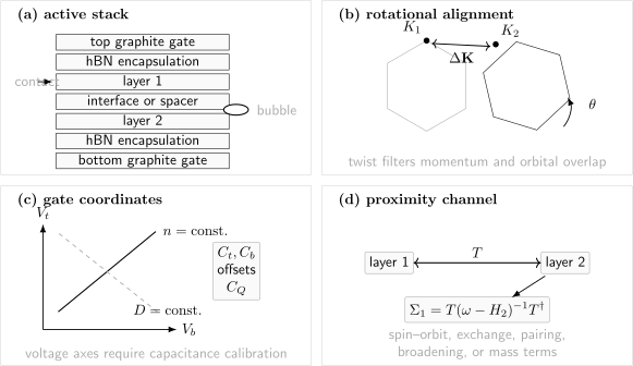
The heterostructure ledger. (a) The active stack includes encapsulation, gates, contacts, spacers, and contamination pockets as well as the target layers. (b) Relative rotation changes the reciprocal-space mismatch and hence momentum-selective tunneling. (c) Top and bottom gates span density-like and displacement-like voltage directions only after capacitance and offset calibration. (d) Integrating out a neighboring layer produces a self-energy whose operator content identifies the proximity channel.
Band alignment is an interface property
Section titled “Band alignment is an interface property”Type-I, type-II, and type-III labels organize whether electron and hole band edges favor the same layer, opposite layers, or an overlapping broken-gap arrangement. They are useful starting points, not immutable properties of two isolated materials. The assembled interface can acquire:
- an interface dipole and vacuum-level shift;
- strain-dependent band edges;
- quasiparticle self-energy changes from the dielectric environment;
- hybridization and anticrossings;
- charge-transfer doping and electrostatic band bending;
- field- and density-dependent many-body renormalization.
Consequently, subtracting tabulated electron affinities does not establish the operating-device alignment. Photoemission, scanning tunneling spectroscopy, optical transitions, transport thresholds, capacitance, and first-principles calculations constrain different quantities. A defensible alignment combines compatible probes under a stated density, field, temperature, and interface condition.
Clean does not mean featureless
Section titled “Clean does not mean featureless”Dry pickup can keep polymer away from an internal interface, but it does not guarantee a uniform one. Hydrocarbons, adsorbed water, and air can aggregate into bubbles as the surrounding regions self-clean. Wrinkles, folds, tears, edge debris, trapped particles, and transfer-induced strain remain possible. Annealing or mechanical cleaning can improve large areas while also moving bubbles, changing strain, or damaging sensitive layers.
The physically active region must be located rather than assumed. Useful checks include optical and atomic-force microscopy, Raman strain and doping maps, photoluminescence maps, transmission electron microscopy where appropriate, scanning probes, and spatially resolved transport or microwave response. A high mobility averaged over one path does not prove that every interface region is uniform.
Twist Angle and Alignment
Section titled “Twist Angle and Alignment”Rotation controls momentum communication
Section titled “Rotation controls momentum communication”Let and denote corresponding crystal momenta in two layers. Relative rotation creates the mismatch
In an ideal translationally invariant interface, elastic tunneling obeys momentum matching modulo reciprocal vectors,
Twist can therefore suppress, enable, or resonantly tune tunneling between particular valleys and Fermi contours. Disorder, phonons, finite device size, and a moiré reciprocal lattice broaden or supplement the momentum-transfer channels. The observation of current does not by itself mean that bare in-plane momentum was conserved.
Relative translation also matters at atomic registry, and nonuniform strain makes the local angle and mismatch position dependent. For small-angle structures, lattice relaxation can produce large stacking domains separated by solitons. A single nominal twist number is then only the beginning of the structural description.
Alignment is measured, not inferred from a straight edge
Section titled “Alignment is measured, not inferred from a straight edge”Crystallographic edges can be armchair, zigzag, reconstructed, faceted, or unrelated to a visible cleavage line. Better alignment evidence may come from:
| method | constrains | limitation |
|---|---|---|
| polarization-resolved second-harmonic generation | crystal axes in suitable noncentrosymmetric layers | layer parity, interference, and optical spot averaging |
| Raman spectroscopy | stacking, strain, and selected rotational signatures | calibration is material and resonance dependent |
| electron or x-ray diffraction | reciprocal-lattice orientation | sample preparation and spatial averaging |
| scanning probe moiré imaging | local period, orientation, and reconstruction | local field of view need not represent the whole device |
| transport or tunneling resonance | momentum-space alignment of active states | also depends on density, disorder, bias, and contacts |
Report the method, angular uncertainty, and spatial scale. A global angle from diffraction and a local angle from microscopy can legitimately differ when heterostrain or relaxation is present.
Dynamic rotation experiments show that angle can be a device control rather than a fabrication constant. They also reveal friction, pinning, hysteresis, and structural relaxation. “Twist-tunable” should therefore specify whether angle was changed in situ, inferred across several devices, or assumed from the assembly geometry.
Encapsulation and Gating
Section titled “Encapsulation and Gating”Encapsulation is an active materials choice
Section titled “Encapsulation is an active materials choice”Hexagonal boron nitride is widely used because it can provide an atomically flat, comparatively low-disorder dielectric and an excellent tunnel barrier. Its role depends on thickness and placement:
- as a substrate, it changes roughness, charge disorder, and screening;
- as a cap, it protects air-sensitive layers and modifies the top dielectric;
- as a spacer, it suppresses tunneling while retaining electrostatic or exchange coupling;
- as a gate dielectric, it sets capacitance and breakdown constraints;
- when crystallographically aligned, it can itself create a moiré perturbation.
It is therefore misleading to call hBN completely inert. Remote phonons, lattice alignment, dielectric screening, defects, trapped charge, and pressure all can affect the active layer. Other encapsulants introduce their own chemical stability, permittivity, phonon, and band-offset ledgers.
The stack determines which voltages are independent
Section titled “The stack determines which voltages are independent”A dual-gated drawing suggests separate control of total density and transverse displacement, but the actual map from voltages to layer densities is a capacitance problem. Geometric capacitances, quantum capacitance, contact potentials, screening by nearby graphite, trapped charge, and leakage all enter. In a multilayer device, each conducting sheet can have a distinct electrochemical potential.
Two-Dimensional Materials gives the canonical two-gate coordinate convention. In a more general stack, write a capacitance matrix,
then close it with the material relation between and chemical potential . Treating every sheet as a perfect metal removes quantum-capacitance and layer-polarization physics precisely where it may be most important.
Good gate coordinates are verified experimentally. Charge neutrality, Landau filling, capacitance, compressibility, optical oscillator transfer, or a known commensurate density can provide anchors. Constant-density and constant-displacement sweeps should be stated in calibrated coordinates, not merely as diagonal lines on an arbitrary two-voltage plot.
Contacts define the open system
Section titled “Contacts define the open system”Top contacts can damage or dope an exposed surface; edge contacts can access an encapsulated conductor; graphene contacts can be electrostatically tuned; tunnel contacts trade invasiveness for resistance. In semiconducting layers, Schottky barriers and contact-gate regions can dominate two-terminal behavior. In vertical devices, the electrodes are also part of the tunneling spectral function.
A device interpretation should separate channel, contact, and leakage contributions by using four-terminal measurements where possible, multiple contact pairs, length scaling, bias dependence, and gate-selective contact control. A resistance peak may belong to the channel, an injection barrier, a depleted lead, or a parallel path.
Proximity Effects
Section titled “Proximity Effects”Integrating out a layer exposes the mechanism
Section titled “Integrating out a layer exposes the mechanism”For
the Green function projected onto layer 1 is
Read from right to left, this proximity self-energy sends a layer-1 state into layer 2 through the adjoint tunneling matrix , propagates it at frequency with the resolvent , and returns it through . The sequence makes clear that the inherited operator structure depends jointly on tunneling selection rules and the neighboring layer’s spectrum.
The matrix structure of can induce spin–orbit terms, exchange fields, layer or sublattice masses, pairing amplitudes in Nambu space, velocity changes, and lifetime broadening. This formula describes hybridization-mediated proximity. It does not include every interfacial effect: static charge transfer, dielectric screening, remote Coulomb coupling, and strain can act even when coherent tunneling is negligible.
For two off-resonant levels with detuning ,
The inherited energy scale and foreign-layer weight increase as detuning decreases. That gives a recurring tradeoff: stronger proximity often comes with more hybridization, scattering, or loss of the original layer identity. Large fitted proximity parameters should be checked against observed anticrossings, linewidths, and spectral-weight transfer.
Name the channel before naming the effect
Section titled “Name the channel before naming the effect”| claimed proximity | microscopic channel to test | discriminating evidence |
|---|---|---|
| spin–orbit | spin-dependent hybridization and broken interface symmetry | spin-precession anisotropy, weak-antilocalization controls, band splitting |
| magnetic exchange | virtual hopping or exchange across the interface | field and magnetization hysteresis, thickness dependence, domain correlation |
| superconducting | coherent pair amplitude through a transparent interface | Andreev spectra, Josephson current, phase and field interference |
| dielectric | modified screened interaction without substantial tunneling | spacer and dielectric-thickness dependence, quasiparticle and optical shifts |
| phonon | interlayer or substrate vibrational coupling | isotope, temperature, resonance, and linewidth response |
| charge-transfer | chemical-potential equilibration and interface dipole | work-function, core-level, density, and gate-reversal measurements |
The neighboring material can also introduce disorder, stray fields, strain, heating, or parallel conduction that mimics the target response. A proximity claim becomes persuasive when it tracks the source layer’s state, decays or evolves with spacer thickness, follows symmetry, and survives electrostatic and contact controls.
Spin–Orbit Coupling in Solids owns the general spin Hamiltonians. Exchange Interactions owns magnetic coupling mechanisms. Superconducting Proximity Effect owns bulk real-space anomalous propagation, inverse proximity, and clean or diffusive coherence through the stack. Proximity and Andreev Physics owns BTK interface scattering, few-mode Andreev levels, and hybrid-device evidence.
Device Tunability
Section titled “Device Tunability”Vertical tunneling is a spectral-overlap measurement
Section titled “Vertical tunneling is a spectral-overlap measurement”In a weak-tunneling description, the current between two electrodes can be organized as
The spectral functions include band structure, lifetime, and interactions. The matrix element contains barrier thickness, orbital overlap, twist, and momentum selection. Gates can tune density and relative alignment; bias changes the energy window. Resonant spectral overlap can produce a current peak and negative differential conductance, but series resistance, heating, charge trapping, and circuit instability must be excluded.
For a simple barrier estimate,
One extra atomic spacer can therefore change current by orders of magnitude. The formula is only a scaling guide: real hBN and semiconductor barriers have crystalline bands, momentum filtering, defects, image potentials, and bias-dependent profiles.
Tunability is multidimensional
Section titled “Tunability is multidimensional”| control | primary target | frequent confounder |
|---|---|---|
| material sequence | band offsets and available proximity channels | trapped interfaces and changed contacts |
| twist and translation | momentum matching and local registry | relaxation, heterostrain, spatial variation |
| spacer thickness | tunneling and exchange strength | pinholes, thickness steps, defect-assisted current |
| density and displacement | chemical potential and layer polarization | quantum capacitance and contact depletion |
| interlayer bias | spectral alignment and vertical current | Joule heating and charge traps |
| pressure | interlayer distance and hybridization | strain and irreversible slippage |
| optical drive | carrier and exciton populations | heating and nonequilibrium screening |
| magnetic state | exchange and spin filtering | domains, stray fields, hysteresis |
The strongest device claims follow a closed loop: a calibrated control changes a predicted Hamiltonian term, an appropriate observable responds with the expected symmetry and scale, and independent measurements exclude contact, thermal, and structural alternatives.
Experimental Claim Ladder
Section titled “Experimental Claim Ladder”- Identify every layer. Record composition, polytype, thickness, sequence, and air exposure.
- Map the active interfaces. Locate bubbles, wrinkles, strain, cracks, and clean regions rather than relying on an optical outline.
- Measure alignment. Give the method, angular uncertainty, and local or global spatial scale.
- Close electrostatics and contacts. Calibrate density, displacement, quantum capacitance, leakage, and injection barriers.
- Separate coupling channels. Test hybridization, charge transfer, dielectric response, strain, and heating before assigning proximity.
- Match the probe to the claim. Use anticrossings for coherent mixing, thermodynamics for incompressibility, phase-sensitive probes for superconductivity, and spatial correlation for domains.
- Report reproducibility and hysteresis. Compare regions, contact pairs, devices, sweep directions, and thermal cycles.
Common Mistakes
Section titled “Common Mistakes”Treating van der Waals bonding as zero interlayer coupling
Section titled “Treating van der Waals bonding as zero interlayer coupling”Weak adhesion relaxes epitaxial constraints; it does not set tunneling, Coulomb, phonon, or exchange coupling to zero.
Assuming encapsulation guarantees a pristine interface
Section titled “Assuming encapsulation guarantees a pristine interface”Bubbles, residue, wrinkles, strain, defects, and edge contamination can remain. Cleanliness is measured region by region.
Assigning twist from flake edges alone
Section titled “Assigning twist from flake edges alone”Visible edges are not guaranteed crystallographic axes. Use a calibrated structural, optical, or electronic alignment probe.
Calling every spectral shift hybridization
Section titled “Calling every spectral shift hybridization”Strain, doping, screening, interface dipoles, and heating also move peaks. Coherent mixing should exchange character or produce a controlled anticrossing.
Treating gate voltage as a layer density
Section titled “Treating gate voltage as a layer density”Multigate stacks require capacitance, quantum-capacitance, offset, and contact calibration. A voltage axis is not yet a thermodynamic coordinate.
Calling every inherited response proximity
Section titled “Calling every inherited response proximity”Parallel conduction, fringe fields, contact changes, and charge transfer can mimic an interfacial effect. Name and test the microscopic channel.
Exercises
Section titled “Exercises”Exercise 1: avoided crossing and layer character
Section titled “Exercise 1: avoided crossing and layer character”For two layer-localized levels with , , and real tunneling , find the eigenenergies. What gap appears at , and what happens to layer character as changes sign?
Solution
Substitution into the two-level spectrum gives
At resonance,
For , each eigenstate is localized mainly in one layer. Sweeping through zero continuously exchanges the dominant layer character between the two branches. Observing both the anticrossing and this character exchange distinguishes coherent mixing from two unrelated crossing resonances.
Exercise 2: momentum matching under twist
Section titled “Exercise 2: momentum matching under twist”Two clean layers have circular Fermi contours of radius whose centers differ by . Ignoring reciprocal-lattice and phonon assistance, when can states at the Fermi energy tunnel elastically? What broadens the condition in a real device?
Solution
Elastic, momentum-conserving tunneling requires the two circles to intersect after one is displaced by . Equal-radius circles intersect when
At equality they touch at one point; below it they intersect at two points. Finite lifetime, temperature, disorder, finite device size, phonons, moiré reciprocal vectors, and density inhomogeneity broaden or add momentum channels. A smooth onset is therefore not automatically evidence against momentum-sensitive tunneling.
Exercise 3: one extra spacer layer
Section titled “Exercise 3: one extra spacer layer”Suppose with . Estimate the current ratio after adding of an otherwise identical barrier.
Solution
At fixed spectral alignment, current scales with , so
The simple model predicts a reduction by about a factor of . A much weaker thickness dependence can signal defects, pinholes, inelastic channels, or a barrier model outside the WKB-like regime.
Exercise 4: dual-gate trajectories
Section titled “Exercise 4: dual-gate trajectories”Use the convention and , with offsets suppressed. If and , find along constant density and constant displacement.
Solution
At constant density,
so
At constant displacement,
and therefore
These are geometric-capacitance slopes. Quantum capacitance, trapped charge, or another conducting layer can curve or shift the experimental trajectories.
Exercise 5: off-resonant proximity scale
Section titled “Exercise 5: off-resonant proximity scale”A layer-1 state couples to a remote layer-2 state with and detuning . Estimate the magnitude of the layer-1 energy shift and the layer-2 spectral weight.
Solution
Convert the detuning to . The shift magnitude is
The foreign-layer weight is approximately
The sign of follows the sign of . The estimate shows how a measurable induced scale can coexist with predominantly layer-1 character.
Exercise 6: audit a spin–orbit proximity claim
Section titled “Exercise 6: audit a spin–orbit proximity claim”A graphene/TMD stack develops a broader weak-antilocalization cusp than a reference graphene device. The authors report proximity-induced spin–orbit coupling. List five checks needed before treating that mechanism as established.
Solution
Useful checks include:
- fit the correct dimensional and intervalley-scattering regime rather than a generic one-parameter cusp;
- measure temperature, density, and field-range dependence to separate dephasing and classical magnetoresistance;
- compare covered and uncovered regions or devices with controlled interface thickness and cleanliness;
- test spin transport or spin-lifetime anisotropy independently of charge magnetoconductance;
- exclude parallel conduction, TMD contact effects, fringe fields, and charge-transfer disorder;
- look for gate, twist, or spacer dependence predicted by the hybridization model.
Weak antilocalization is consistent with enhanced spin relaxation, but one curve does not uniquely determine the operator, magnitude, or interfacial origin of the coupling.
Key Takeaways
Section titled “Key Takeaways”- Van der Waals assembly relaxes lattice matching but does not remove tunneling, electrostatic, strain, phonon, or exchange coupling.
- Layer sequence, interface cleanliness, twist, translation, gates, spacers, and contacts all enter the operative Hamiltonian.
- Coherent hybridization is best identified by controlled anticrossings and exchanged state character, not by a spectral shift alone.
- Alignment must be measured with a stated uncertainty and spatial scale; visible edges are not sufficient.
- Encapsulation can reduce disorder while also changing screening, phonons, tunneling, and moiré coupling.
- A proximity effect needs a named microscopic channel and controls against charge transfer, strain, heating, contacts, and parallel conduction.
- Vertical current measures spectral overlap weighted by a strongly geometry- and momentum-dependent tunneling matrix element.
Connections
Section titled “Connections”- Two-Dimensional Materials owns generic screening, band-alignment taxonomy, optical gaps, and device electrostatics.
- Transition-Metal Dichalcogenides develops the material-specific spin–valley, exciton, and TMD moiré ledgers.
- 2D Magnets and Ferroelectrics owns stacking-dependent interlayer exchange, sliding polarization, and the evidence needed for magnetic, ferroelectric, and magnetoelectric proximity claims.
- Engineered Heterostructures compares van der Waals stacks with epitaxial, oxide, and cavity interfaces through a common transfer-and-loss ledger.
- Device Fabrication Concepts places assembly, encapsulation, contacts, gates, process metrology, cryogenic packaging, and yield inside a cross-platform provenance workflow.
- Graphene applies substrate, mass, strain, and interlayer perturbations to the graphene Dirac basis.
- Twisted Bilayer Graphene develops the small-angle continuum model and the evidence hierarchy for the resulting correlated, superconducting, and topological phases.
- Quantum Wells provides the lattice-matched epitaxial comparison for confinement and band engineering.
- Quantum Tunneling and Transfer-Matrix Method own elementary and multilayer barrier transmission.
- Spin–Orbit Coupling in Solids classifies spin-dependent interface terms and their transport signatures.
- Proximity and Andreev Physics owns BTK interface scattering, few-mode Andreev levels, and mesoscopic device evidence.
- Band Theory Overview separates independent-particle bands from dressed quasiparticle spectra.
Further Reading
Section titled “Further Reading”- A. K. Geim and I. V. Grigorieva, “Van der Waals Heterostructures,” Nature 499, 419–425 (2013), doi:10.1038/nature12385.
- K. S. Novoselov, A. Mishchenko, A. Carvalho, and A. H. Castro Neto, “2D Materials and van der Waals Heterostructures,” Science 353, aac9439 (2016), doi:10.1126/science.aac9439.
References
Section titled “References”- K. S. Novoselov et al., “Two-Dimensional Atomic Crystals,” Proceedings of the National Academy of Sciences 102, 10451–10453 (2005), doi:10.1073/pnas.0502848102.
- C. R. Dean et al., “Boron Nitride Substrates for High-Quality Graphene Electronics,” Nature Nanotechnology 5, 722–726 (2010), doi:10.1038/nnano.2010.172.
- L. Britnell et al., “Field-Effect Tunneling Transistor Based on Vertical Graphene Heterostructures,” Science 335, 947–950 (2012), doi:10.1126/science.1218461.
- L. A. Ponomarenko et al., “Cloning of Dirac Fermions in Graphene Superlattices,” Nature 497, 594–597 (2013), doi:10.1038/nature12187.
- C. R. Dean et al., “Hofstadter’s Butterfly and the Fractal Quantum Hall Effect in Moiré Superlattices,” Nature 497, 598–602 (2013), doi:10.1038/nature12186.
- L. Wang et al., “One-Dimensional Electrical Contact to a Two-Dimensional Material,” Science 342, 614–617 (2013), doi:10.1126/science.1244358.
- W. J. Yu et al., “Highly Efficient Gate-Tunable Photocurrent Generation in Vertical Heterostructures of Layered Materials,” Nature Nanotechnology 8, 952–958 (2013), doi:10.1038/nnano.2013.219.
- A. Mishchenko et al., “Twist-Controlled Resonant Tunnelling in Graphene/Boron Nitride/Graphene Heterostructures,” Nature Nanotechnology 9, 808–813 (2014), doi:10.1038/nnano.2014.187.
- C.-H. Lee et al., “Atomically Thin p–n Junctions with van der Waals Heterointerfaces,” Nature Nanotechnology 9, 676–681 (2014), doi:10.1038/nnano.2014.150.
- C. R. Woods et al., “Commensurate–Incommensurate Transition in Graphene on Hexagonal Boron Nitride,” Nature Physics 10, 451–456 (2014), doi:10.1038/nphys2954.
- A. V. Kretinin et al., “Electronic Properties of Graphene Encapsulated with Different Two-Dimensional Atomic Crystals,” Nano Letters 14, 3270–3276 (2014), doi:10.1021/nl5006542.
- M.-H. Chiu et al., “Determination of Band Alignment in the Single-Layer MoS/WSe Heterojunction,” Nature Communications 6, 7666 (2015), doi:10.1038/ncomms8666.
- P. Rivera et al., “Observation of Long-Lived Interlayer Excitons in Monolayer MoSe–WSe Heterostructures,” Nature Communications 6, 6242 (2015), doi:10.1038/ncomms7242.
- F. Withers et al., “Light-Emitting Diodes by Band-Structure Engineering in van der Waals Heterostructures,” Nature Materials 14, 301–306 (2015), doi:10.1038/nmat4205.
- V. E. Calado et al., “Ballistic Josephson Junctions in Edge-Contacted Graphene,” Nature Nanotechnology 10, 761–764 (2015), doi:10.1038/nnano.2015.156.
- K. Kim et al., “van der Waals Heterostructures with High Accuracy Rotational Alignment,” Nano Letters 16, 1989–1995 (2016), doi:10.1021/acs.nanolett.5b05263.
- Z. Wang et al., “Origin and Magnitude of ‘Designer’ Spin–Orbit Interaction in Graphene on Semiconducting Transition Metal Dichalcogenides,” Physical Review X 6, 041020 (2016), doi:10.1103/PhysRevX.6.041020.
- T. S. Ghiasi, J. Ingla-Aynés, A. A. Kaverzin, and B. J. van Wees, “Large Proximity-Induced Spin Lifetime Anisotropy in Transition-Metal Dichalcogenide/Graphene Heterostructures,” Nano Letters 17, 7528–7532 (2017), doi:10.1021/acs.nanolett.7b03460.
- R. Ribeiro-Palau et al., “Twistable Electronics with Dynamically Rotatable Heterostructures,” Science 361, 690–693 (2018), doi:10.1126/science.aat6981.
- D. G. Purdie et al., “Cleaning Interfaces in Layered Materials Heterostructures,” Nature Communications 9, 5387 (2018), doi:10.1038/s41467-018-07558-3.