Topological Insulators
A time-reversal-invariant electronic topological insulator is a bulk-gapped, charge-conserving phase with spinful time reversal whose occupied states have a nontrivial obstruction to a symmetric atomic limit. In two dimensions this is the quantum spin Hall phase, with an odd number of helical Kramers pairs at an edge. In three dimensions a strong topological insulator has an odd surface Dirac-cone parity.
In broad taxonomy, a Chern insulator is also a topological band insulator. Here the shorter phrase topological insulator means the spinful, time-reversal-invariant class unless another symmetry setting is named. This keeps its structure separate from the broken-time-reversal integer Hall case.
The definition concerns the bulk phase, not whether a finite sample has infinite resistance. A real crystal can be topologically nontrivial yet conduct through doped bulk bands, surface accumulation layers, contacts, or sidewalls. Conversely, a trivial surface resonance can conduct without implying a nontrivial bulk invariant.
The occupied-projector formulas below apply directly to noninteracting systems and to materials with a controlled quasiparticle-band description. Interacting descendants can retain the same symmetry-protected distinction, but then a Green-function, flux-insertion, response, or other many-body diagnostic must replace a naive product of one-electron parity eigenvalues.
This page owns the class-AII invariant, quantum spin Hall boundary physics, strong and weak three-dimensional indices, surface Dirac cones, benchmark materials, and the evidence needed to connect them. Topology in Quantum Matter owns the general phase-equivalence and evidence framework; Time Reversal for Spin-1/2 Particles and Kramers Degeneracy own the antiunitary algebra; Spin–Orbit Coupling in Solids owns microscopic spin–orbit mechanisms; and Chern Numbers in Band Theory owns the charge-Chern formalism.
Required background. Bloch’s Theorem supplies the band subspace, Time Reversal for Spin-1/2 Particles and Kramers Degeneracy supply the class-AII algebra, and Topology in Quantum Matter supplies the deformation and evidence framework.
Helpful background. Spin–Orbit Coupling in Solids supplies the microscopic band mechanism, and Chern Numbers in Band Theory supplies the charge-Chern comparison.
Insulating Bulk, Conducting Boundary
Section titled “Insulating Bulk, Conducting Boundary”Consider a periodic one-electron or quasiparticle Hamiltonian with chemical potential . The clean bulk is spectrally insulating when
and lies in that indirect gap. A positive direct gap at every momentum is needed to define a smooth occupied projector,
but a material can have a direct gap while valence and conduction energies overlap indirectly. Such a system is not a bulk transport insulator at charge neutrality.
The topological question asks whether can be deformed to an atomic-insulator projector while preserving:
- the occupied–empty separation;
- charge conservation;
- spinful time reversal;
- locality and the lattice setting;
- any additional assumptions used by the chosen diagnostic.
For the nontrivial phase, a boundary with a trivial, symmetry-preserving vacuum cannot be everywhere featureless in the same low-energy description. In a clean noninteracting system it carries gapless states connecting valence and conduction bands. The boundary spectrum can move, bend, acquire extra trivial pairs, or merge into projected bulk continua. What cannot change without closing the bulk gap or relaxing the protection is the parity of the protected boundary structure.
This is why the phrase “insulating bulk, conducting boundary” is useful but incomplete. It does not promise:
- a universal three-dimensional surface conductivity;
- a chemical potential exactly at the Dirac point;
- absence of all scattering;
- immunity to magnetic order or finite-size hybridization;
- negligible parallel bulk conduction;
- dissipationless transport at arbitrary temperature and length.
Time-Reversal Symmetry
Section titled “Time-Reversal Symmetry”For spinful electrons without magnetic order or external time-reversal breaking,
In a spin-only basis one may choose , but in a multiorbital crystal acts on the full Bloch spinor. The Pauli matrices used in an effective model need not equal the microscopic spin operator unless that identification is stated.
Time-reversal-invariant momenta
Section titled “Time-reversal-invariant momenta”A crystal momentum is time-reversal invariant when
for a reciprocal-lattice vector . Equivalently,
These points are called TRIM. A two-dimensional Brillouin torus has four TRIM, and a three-dimensional one has eight. At each TRIM, every spinful Bloch eigenstate has an orthogonal Kramers partner at the same energy.
Away from a TRIM, time reversal pairs a state at with one at . Spin–orbit coupling may split bands at a generic momentum when inversion is absent, but Kramers degeneracy remains at the TRIM. If both inversion and time reversal are present, every band is doubly degenerate at every .
Symmetry of Bloch States owns the crystalline little-group labels and the Kramers, , and symmetry-enforced degeneracy conditions used here. This page begins after that representation data and owns the invariant, parity and Wilson-loop diagnostics, and boundary consequences.
Why the Chern number vanishes but topology survives
Section titled “Why the Chern number vanishes but topology survives”Time reversal sends the occupied trace Berry curvature to
Therefore the net occupied charge Chern number vanishes:
The vanishing integer says that equilibrium charge Hall conductivity is forbidden. It removes the Chern obstruction to some exponentially localized Wannier basis, but it does not construct a globally time-reversal-compatible basis for each Kramers pair. In the nontrivial phase, the obstruction is specifically to a time-reversal-covariant, Kramers-paired Wannier frame, not to exponential localization after that gauge condition is relaxed. Wannier Functions owns this basis-level distinction and its construction. The remaining obstruction has only two values, trivial or nontrivial, and is measured by a invariant.
The Z₂ Invariant
Section titled “The Z₂ Invariant”Partner switching
Section titled “Partner switching”Imagine following occupied Kramers pairs from one TRIM to another. In a trivial insulator, partners can be chosen so that they reconnect without an odd exchange. In a quantum spin Hall insulator, the pairing switches an odd number of times. Adding two identical nontrivial copies permits the switches to recombine, which is the physical origin of
The invariant is thus a parity, not a small Chern number. It remains meaningful when spin is not conserved and “spin-up band” is not globally defined.
Sewing-matrix formulation
Section titled “Sewing-matrix formulation”Choose a smooth occupied frame locally and define the sewing matrix
At a TRIM, is antisymmetric:
Its Pfaffian is therefore defined. With a globally consistent choice of square-root branches, set
For a two-dimensional insulator,
Individual values in this gauge-general formula are not arbitrary observables. The branch-consistent product is the invariant. A calculation that independently chooses square-root signs at each TRIM can manufacture a false answer.
Inversion-symmetry shortcut
Section titled “Inversion-symmetry shortcut”If inversion is also a symmetry and commutes with , the two states in each occupied Kramers pair share one parity eigenvalue
For occupied Kramers pairs, define
The same two-dimensional product gives . This is the Fu–Kane parity criterion. It is powerful because it uses only symmetry eigenvalues at the TRIM, but it is valid only while inversion symmetry is present. “Band inversion” at one momentum is suggestive, not a substitute for the complete parity product or another gauge-invariant diagnostic.
Wilson-loop formulation
Section titled “Wilson-loop formulation”For numerical work without inversion, one may form an occupied-subspace Wilson loop, schematically
Its eigenphases are hybrid-Wannier centers modulo a lattice period. Time reversal constrains them into Kramers pairs at and . An odd partner switch, equivalently an odd crossing of a reference line during half of the cycle, gives . The spectrum of is gauge invariant even though the chosen occupied frame is not.
The invariant can change only if the occupied subspace ceases to be well defined, usually through a bulk gap closing, or if time reversal is broken so that the classifying problem changes. A surface gap closing alone does not necessarily change the three-dimensional bulk index. Topological Phase Transitions owns the general direct-gap, parity-switch, gapless-intermediate, disorder, and interaction mechanisms.
Quantum Spin Hall Effect
Section titled “Quantum Spin Hall Effect”Two opposite Chern sectors
Section titled “Two opposite Chern sectors”In the artificial limit where is conserved, a quantum spin Hall state can be pictured as two Chern insulators related by time reversal:
The charge Chern number cancels,
while
This picture is excellent intuition, but it is not the general definition. Rashba coupling mixes spin sectors, physical spin is not conserved, and spin Hall conductivity need not remain exactly quantized. The invariant and helical edge anomaly survive as long as the bulk gap and time reversal survive.
The Bernevig–Hughes–Zhang model
Section titled “The Bernevig–Hughes–Zhang model”A continuum model for HgTe/CdTe quantum wells uses an electron-like and hole-like orbital doublet in two time-reversed blocks:
with
The orbital Pauli matrices are ; the block label is exchanged by time reversal. In the regularized continuum model, the mass near has sign , while the large- mass has sign . The nontrivial regime has opposite signs:
At the gap closes and the index can change. In HgTe/CdTe wells, changing the well thickness reverses the order of the electron-like and heavy-hole-like subbands. The experimentally important critical thickness is about , though its precise value is structure dependent.
The condition belongs to this regularized model and convention. The sign of one fitted “mass” without the ultraviolet completion, orbital basis, and convention is not a universal invariant.
Helical edge states
Section titled “Helical edge states”Across an interface between topological and trivial masses, the effective mass changes sign and a Kramers pair localizes at the boundary. Time reversal exchanges its counterpropagating branches and enforces a crossing at an edge TRIM. Edge and Surface States owns the minimal Hamiltonian, Kramers backscattering proof, helical Luttinger description, finite-width hybridization, and boundary-transport evidence ladder.
The phase-specific statement here is parity: ordinary boundary bands can add or remove an even number of helical pairs, but one anomalous pair remains while the two-dimensional bulk and time reversal remain intact.
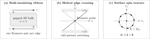
The boundary ledger. A two-dimensional bulk supports counterpropagating partners on each edge; an odd helical pair must cross at a time-reversal-invariant edge momentum; and a simple strong-topological-insulator surface has a single constant-energy contour with tangential spin–momentum locking. Extra trivial pairs may be added, but the protected parity cannot change without altering the bulk or its protection assumptions.
Conductance and interactions
Section titled “Conductance and interactions”An ideal short strip can approach because its two edges conduct in parallel. The measured value depends on geometry, equilibration, contacts, edge length, and bulk leakage, so it is supporting evidence rather than the invariant itself. Interactions can enable multiparticle processes or boundary symmetry breaking without invalidating the bulk phase label.
Three-Dimensional Topological Insulators
Section titled “Three-Dimensional Topological Insulators”Four bulk indices
Section titled “Four bulk indices”Let be primitive reciprocal vectors. The eight TRIM are
For an inversion-symmetric system, compute the parity product at each TRIM. The strong index is
and the three weak indices obey
The phase label is conventionally written
A strong topological insulator has . In a clean noninteracting boundary description it has an odd number of surface Dirac cones, independent of surface orientation. Time-reversal-preserving disorder cannot remove the strong parity while a mobility gap and the bulk phase survive.
A weak topological insulator has but at least one nonzero weak index. It can be viewed heuristically as stacked quantum spin Hall layers. Its clean side surfaces can carry an even number of Dirac cones, while other surfaces may be gapped. The weak vector depends on lattice translation structure and is more vulnerable to translation-breaking disorder, although dislocations and selected surfaces can retain characteristic modes.
Magnetoelectric angle
Section titled “Magnetoelectric angle”The strong index also appears in the bulk electromagnetic response through an angle defined modulo . Time reversal sends to , so a time-reversal-invariant insulator permits
The strong phase has . If a surface is gapped by time-reversal breaking and the chemical potential lies in that gap, its Hall response is half-integer modulo an added integer quantum Hall layer:
The half-integer sign is fixed by the oriented surface mass, while the integer reflects an attached quantum Hall layer or equivalent boundary convention. This is not the dc Hall conductivity of an ordinary gapless surface. Measuring the topological magnetoelectric response requires control of all surfaces, magnetic domains, side conduction, and the chemical potential.
Surface Dirac Cones
Section titled “Surface Dirac Cones”The strong index requires odd surface-cone parity in a clean noninteracting description. Edge and Surface States owns the minimal Dirac Hamiltonian, spin–pseudospin texture, magnetic mass, warping, exact-backscattering rule, thin-film hybridization, and probe limitations.
For the bulk phase, three qualifications matter. Opposite surfaces of a finite film can pair and gap while preserving time reversal. Rashba-split accumulation layers and dangling-bond states can coexist with the anomalous cone. Strong interactions can replace a gapless cone by symmetry-preserving intrinsic surface topological order. None of these options turns one isolated anomalous surface into an ordinary, unique, symmetry-preserving band insulator.
Material Examples
Section titled “Material Examples”Evidence ladder
Section titled “Evidence ladder”A trustworthy identification combines bulk, boundary, symmetry, and transport information.
| Claim | Strong evidence package | Insufficient by itself |
|---|---|---|
| nontrivial bulk band topology | bulk gap plus parity, Wilson-loop, or equivalent invariant from a validated occupied subspace | one inverted orbital ordering |
| quantum spin Hall edge | perimeter-localized conduction, nonlocal geometry, length and contact scaling, magnetic-field control, bulk insulation | one residual conductance plateau |
| strong-TI surface cone | surface localization, negligible dispersion, odd partner switching, compatible spin texture and bulk invariant | a generic linear surface band |
| surface-dominated transport | gating, thickness, Hall, oscillation, and carrier-density consistency excluding bulk channels | weak antilocalization alone |
| time-reversal protection | controlled comparison of nonmagnetic and magnetic perturbations with gap and scattering analysis | absence of one scattering wavevector |
Angle-resolved photoemission can map surface dispersion and photon-energy dependence; spin-resolved measurements constrain texture. Scanning tunneling spectroscopy resolves local gaps, standing waves, and edge localization. Transport tests whether those states carry current in a bulk-insulating regime. First-principles calculations connect orbital character to an invariant, but surface band bending, disorder, and the actual chemical potential remain experimental inputs.
Benchmark platforms
Section titled “Benchmark platforms”| Platform | Dimension and phase | Best-established evidence | Persistent limitation |
|---|---|---|---|
| HgTe/CdTe quantum wells | 2D quantum spin Hall | thickness-driven inversion, short-device conductance near , edge and magnetic-field dependence | long edges show inelastic scattering, puddles, and contact sensitivity |
| monolayer - | 2D quantum spin Hall | bulk-gap spectroscopy, edge conduction, short-edge quantization reported up to about | edge resistance and zero-bias anomalies require interaction and disorder modeling |
| bismuthene on SiC | large-gap 2D candidate | approximately spectroscopic gap and edge-localized states consistent with theory | transport quantization and protection tests are less complete |
| 3D strong topological insulator | bulk gap and odd surface-state connectivity by ARPES | alloy disorder and complex surface spectrum complicate transport | |
| , , | 3D strong topological insulators | simple single-cone prediction, ARPES observation, spin texture, scanning-probe evidence | vacancies, antisites, band bending, and bulk carriers often dominate devices |
| - | weak-topological-insulator platform | surface-dependent Dirac structure compatible with weak indices | termination, small crystals, and side-surface access complicate verification |
The first five rows are not at one identical evidential stage. HgTe and the bismuth-chalcogenide strong topological insulators are benchmark phases, while every device still has nonuniversal transport. Monolayer has unusually strong combined evidence for a van der Waals quantum spin Hall platform, but its interacting edge is not an ideal noninteracting wire. Bismuthene illustrates why a large spectroscopic gap and an edge signal should not be promoted directly into a room-temperature, dissipationless-device claim.
Correlated candidates such as , magnetic topological insulators, crystalline topological insulators, and superconducting proximity structures require additional canonical treatments. Their symmetry, quasiparticle, and response assumptions are not interchangeable with the nonmagnetic band-insulator setting developed here.
Status
Section titled “Status”Established theory: the two-dimensional and three-dimensional class-AII classifications, Kramers-protected boundary parity, inversion criterion, and strong-TI surface anomaly.
Established benchmark platforms: quantum spin Hall behavior in inverted HgTe quantum wells and strong-topological-insulator surface bands in the bismuth-antimony and bismuth-chalcogenide families.
Active materials engineering: suppressing bulk carriers, controlling surface chemical potential, extending ballistic helical-edge lengths, raising operating temperatures, and making reproducible magnetic or superconducting interfaces.
Active and model dependent: correlated topological insulators, interacting edge reconstruction, disorder-stabilized regimes, and claims that infer protection from a single transport or spectroscopy signature.
Common Mistakes
Section titled “Common Mistakes”- Calling every spin–orbit-gapped material a topological insulator.
- Treating band inversion at one momentum as the invariant.
- Using inversion parities after inversion symmetry has been broken.
- Concluding that makes every time-reversal-invariant insulator trivial.
- Defining the quantum spin Hall phase by conserved when Rashba coupling is present.
- Saying time reversal forbids all scattering rather than exact elastic backscattering between Kramers partners.
- Calling a conducting surface proof of a bulk topological invariant.
- Calling the bulk metallic because a boundary conducts.
- Expecting a universal 3D surface conductance.
- Ignoring top–bottom hybridization in thin films.
- Treating weak antilocalization or a Berry-phase fit as unique evidence.
- Confusing a short-range-entangled topological band phase with intrinsic topological order and anyons.
Exercises
Section titled “Exercises”1. Locate the two-dimensional TRIM
Section titled “1. Locate the two-dimensional TRIM”For a rectangular lattice with reciprocal vectors and , list all momenta satisfying . Explain why each occupied spinful band is Kramers degenerate there.
Solution
The four inequivalent choices are
Thus the TRIM are
At any one of them, differs from by a reciprocal vector and represents the same crystal momentum. Time reversal therefore maps an eigenstate back into the same momentum sector. Since , Kramers’ theorem makes the partner orthogonal and degenerate.
2. Opposite Chern sectors
Section titled “2. Opposite Chern sectors”In a spin-conserving model, suppose and time reversal gives . Find the charge Chern number and the index. What changes if two identical copies are stacked and allowed to mix without breaking time reversal?
Solution
The charge Chern number is
The quantum spin Hall index is the parity of one spin-sector Chern number:
Two copies add modulo two:
Their two helical Kramers pairs can mix through time-reversal-preserving couplings and gap in pairs. The charge Chern number was zero both before and after stacking, illustrating why it does not diagnose the phase.
3. Use inversion parities in two dimensions
Section titled “3. Use inversion parities in two dimensions”A centrosymmetric insulator has parity products
Find . Would the same four numbers remain a valid shortcut after a polar distortion breaks inversion but leaves the gap and time reversal intact?
Solution
The Fu–Kane product is
so
After inversion is broken, parity is no longer a good quantum number and the shortcut is invalid. If the gap and time reversal remain intact during the distortion, the phase itself cannot change. It must instead be evaluated by a gauge-general method such as sewing-matrix or Wilson-loop partner flow.
4. Diagnose the BHZ mass
Section titled “4. Diagnose the BHZ mass”For the regularized BHZ block with mass , classify the cases and . Why must the transition occur at in this minimal model?
Solution
At , the mass has sign . At large momentum the regularizing term dominates and has sign . The signs are opposite when
so the orbital texture wraps nontrivially and the full time-reversed pair is in the quantum spin Hall phase. For , the signs agree and the phase is trivial.
At , the two orbital sectors meet at :
The occupied projector is then undefined at the touching, allowing the invariant to change. In a lattice model, another symmetry-allowed gap closing elsewhere in the Brillouin zone could also drive a transition.
5. Stable parity under edge reconstruction
Section titled “5. Stable parity under edge reconstruction”A quantum spin Hall edge begins with one helical Kramers pair. Boundary reconstruction adds two further pairs. Explain why time-reversal-symmetric mixing can gap four branches while leaving one pair gapless.
Solution
The reconstructed edge has three Kramers pairs, an odd count. Time-reversal-symmetric couplings can pair two Kramers pairs into a nonanomalous four-branch sector and gap it. One pair remains because there is no second anomalous pair with which to form a completely gapped one-dimensional theory.
The detailed crossing positions and velocities can change, so one need not see the original pair preserved branch by branch. What survives is
Removing the final pair requires time-reversal breaking, coupling to another anomalous boundary, a bulk transition, or an interacting nontrivial boundary option.
6. Strong and weak surface orientation
Section titled “6. Strong and weak surface orientation”Compare a strong topological insulator with a weak topological insulator viewed as stacked quantum spin Hall layers. Which one requires an odd surface-cone parity on every surface orientation, and why can the weak phase have a dark surface?
Solution
A strong topological insulator has . Its anomalous odd-cone parity does not depend on choosing a surface parallel to a stacking direction, although termination can reshape the dispersion or merge it with bulk projections.
A weak phase has and nonzero weak indices. In the stacking picture, side surfaces expose the edges of the layers and can support an even set of surface cones. A surface normal to the stacking direction need not expose those edges and can be gapped. Translation-breaking disorder can also mix the even cone set more readily.
This orientation dependence is why the weak indices and surface normal must accompany a claim about weak-TI boundary modes.
7. Count conductance channels carefully
Section titled “7. Count conductance channels carefully”An ideal short quantum spin Hall strip has one helical Kramers pair on each of its two edges and ideal reservoirs. What two-terminal conductance is expected? Why can a longer device fall below it without changing the bulk invariant?
Solution
Each edge supplies one transmitting channel from the source to the drain and contributes
The two edges are in parallel, so
A longer device can contain charge puddles, extra edge modes, inelastic scattering, multiparticle processes, imperfect contacts, or sections where the chemical potential leaves the bulk gap. These reduce the measured conductance while the bulk index remains unchanged. Conductance quantization tests an operational regime, not just the abstract phase label.
8. Audit a topological-insulator claim
Section titled “8. Audit a topological-insulator claim”A crystal shows a linear surface band in photoemission and a low-field weak-antilocalization cusp. The bulk resistivity remains metallic. The sample is announced as a “perfect surface-only strong topological insulator.” Evaluate the claim and name four missing checks.
Solution
The observations are compatible with spin–orbit-coupled surface conduction, but they do not establish the advertised package. A trivial Rashba surface band can look locally linear, and weak antilocalization occurs broadly in the symplectic class. Metallic bulk resistivity directly contradicts the “surface-only” transport claim unless a quantitative multichannel analysis shows otherwise.
Useful missing checks include:
- demonstrate a bulk direct and indirect gap and locate the chemical potential;
- compute or measure a consistent bulk invariant;
- establish surface localization and negligible photon-energy or dispersion;
- show odd surface-state partner switching between surface TRIM;
- compare thickness, gating, Hall density, and quantum oscillations to separate bulk and surface channels;
- test nonmagnetic versus magnetic perturbations and rule out trivial accumulation layers.
A defensible conclusion would report evidence for a candidate topological surface state while withholding “perfect surface-only” until the transport and bulk ledgers converge.
Connections
Section titled “Connections”- Metals, Insulators, and Semiconductors distinguishes spectral, mobility, Mott, Anderson, and topological meanings of “insulator.”
- Symmetry-Protected Structure Preview owns the general logic of a phase that becomes trivial when its protecting symmetry is relaxed.
- Symmetry Classification Preview places spinful time-reversal insulators in class AII and explains why dimension is part of the classification.
- Integer Quantum Hall Effect is the broken-time-reversal comparison: a charge Chern number and chiral edge replace the index and helical boundary.
- Edge and Surface States owns the minimal helical and surface-Dirac theories, robustness ledger, finite-size effects, and boundary-probe workflow.
- Bulk–Boundary Correspondence develops Kramers crossing parity, stable versus raw mode counts, domain-wall masses, and interacting boundary alternatives.
- Conductance Quantization owns Landauer channels, contacts, imperfect transmission, and the distinction between per channel and a bulk invariant.
- Spintronics develops spin injection, detection, conversion, and device metrics beyond equilibrium spin texture.
- Topological Superconductors replaces occupied-electron-band topology by BdG topology and shows how a proximitized topological-insulator boundary can support Majorana defect modes.
- Engineered Heterostructures develops the interface requirements and evidence hierarchy for magnetic and superconducting proximity on topological boundaries.
- Weyl and Dirac Semimetals contrasts these gapped phases with symmetry-protected bulk point nodes, open surface Fermi arcs, and semimetal transport.
- Symmetry-Protected Topological Phases places class-AII band insulators inside the wider interacting framework of symmetric circuits, anomalous boundaries, stacking, and cobordism.
- Entanglement Spectrum explains the virtual-boundary diagnostic and its limits for free and interacting topological phases.
Further Reading
Section titled “Further Reading”- M. Z. Hasan and C. L. Kane, “Colloquium: Topological Insulators,” Reviews of Modern Physics 82, 3045–3067 (2010), doi:10.1103/RevModPhys.82.3045.
- X.-L. Qi and S.-C. Zhang, “Topological Insulators and Superconductors,” Reviews of Modern Physics 83, 1057–1110 (2011), doi:10.1103/RevModPhys.83.1057.
- B. A. Bernevig and T. L. Hughes, Topological Insulators and Topological Superconductors, Princeton University Press, 2013.
References
Section titled “References”- C. L. Kane and E. J. Mele, “Quantum Spin Hall Effect in Graphene,” Physical Review Letters 95, 226801 (2005), doi:10.1103/PhysRevLett.95.226801.
- C. L. Kane and E. J. Mele, “ Topological Order and the Quantum Spin Hall Effect,” Physical Review Letters 95, 146802 (2005), doi:10.1103/PhysRevLett.95.146802.
- B. A. Bernevig, T. L. Hughes, and S.-C. Zhang, “Quantum Spin Hall Effect and Topological Phase Transition in HgTe Quantum Wells,” Science 314, 1757–1761 (2006), doi:10.1126/science.1133734.
- M. König et al., “Quantum Spin Hall Insulator State in HgTe Quantum Wells,” Science 318, 766–770 (2007), doi:10.1126/science.1148047.
- L. Fu, C. L. Kane, and E. J. Mele, “Topological Insulators in Three Dimensions,” Physical Review Letters 98, 106803 (2007), doi:10.1103/PhysRevLett.98.106803.
- J. E. Moore and L. Balents, “Topological Invariants of Time-Reversal-Invariant Band Structures,” Physical Review B 75, 121306(R) (2007), doi:10.1103/PhysRevB.75.121306.
- L. Fu and C. L. Kane, “Topological Insulators with Inversion Symmetry,” Physical Review B 76, 045302 (2007), doi:10.1103/PhysRevB.76.045302.
- C. Wu, B. A. Bernevig, and S.-C. Zhang, “Helical Liquid and the Edge of Quantum Spin Hall Systems,” Physical Review Letters 96, 106401 (2006), doi:10.1103/PhysRevLett.96.106401.
- C. Xu and J. E. Moore, “Stability of the Quantum Spin Hall Effect: Effects of Interactions, Disorder, and Topology,” Physical Review B 73, 045322 (2006), doi:10.1103/PhysRevB.73.045322.
- X.-L. Qi, T. L. Hughes, and S.-C. Zhang, “Topological Field Theory of Time-Reversal Invariant Insulators,” Physical Review B 78, 195424 (2008), doi:10.1103/PhysRevB.78.195424.
- D. Hsieh et al., “A Topological Dirac Insulator in a Quantum Spin Hall Phase,” Nature 452, 970–974 (2008), doi:10.1038/nature06843.
- H. Zhang et al., “Topological Insulators in , and with a Single Dirac Cone on the Surface,” Nature Physics 5, 438–442 (2009), doi:10.1038/nphys1270.
- Y. Xia et al., “Observation of a Large-Gap Topological-Insulator Class with a Single Dirac Cone on the Surface,” Nature Physics 5, 398–402 (2009), doi:10.1038/nphys1274.
- D. Hsieh et al., “A Tunable Topological Insulator in the Spin Helical Dirac Transport Regime,” Nature 460, 1101–1105 (2009), doi:10.1038/nature08234.
- Y. L. Chen et al., “Experimental Realization of a Three-Dimensional Topological Insulator, ,” Science 325, 178–181 (2009), doi:10.1126/science.1173034.
- Z. Alpichshev et al., “STM Imaging of Electronic Waves on the Surface of : Topologically Protected Surface States and Hexagonal Warping Effects,” Physical Review Letters 104, 016401 (2010), doi:10.1103/PhysRevLett.104.016401.
- D. Kim et al., “Surface Conduction of Topological Dirac Electrons in Bulk Insulating ,” Nature Physics 8, 459–463 (2012), doi:10.1038/nphys2286.
- Z. Fei et al., “Edge Conduction in Monolayer ,” Nature Physics 13, 677–682 (2017), doi:10.1038/nphys4091.
- S. Tang et al., “Quantum Spin Hall State in Monolayer -,” Nature Physics 13, 683–687 (2017), doi:10.1038/nphys4174.
- F. Reis et al., “Bismuthene on a SiC Substrate: A Candidate for a High-Temperature Quantum Spin Hall Material,” Science 357, 287–290 (2017), doi:10.1126/science.aai8142.
- S. Wu et al., “Observation of the Quantum Spin Hall Effect up to 100 Kelvin in a Monolayer Crystal,” Science 359, 76–79 (2018), doi:10.1126/science.aan6003.
- E. Noguchi et al., “A Weak Topological Insulator State in Quasi-One-Dimensional Bismuth Iodide,” Nature 566, 518–522 (2019), doi:10.1038/s41586-019-0927-7.