Scanning Tunneling Microscopy and Spectroscopy
Scanning tunneling microscopy (STM) holds a conducting tip a few ångströms from a conducting surface and regulates the vacuum tunneling current while the tip scans. Scanning tunneling spectroscopy (STS) records the current or differential conductance as the bias is varied at a point, along a line, or across a grid. The same junction can therefore resolve atomic-scale spatial structure and millielectronvolt-scale spectral structure.
Neither output is a direct photograph of atoms or of the local density of states. The recorded current depends exponentially on tip–sample separation and also on the electronic states, tip apex, tunneling matrix element, occupation factors, feedback history, voltage modulation, and instrumental response. Atomic resolution means that the junction is sensitive to atomic-scale electronic structure; it does not make every bright maximum an atomic coordinate.
A useful evidence ladder is:
- controller record: current, applied sample bias, commanded piezo coordinates, feedback error, and time;
- calibrated image or spectrum: height or conductance after scanner, voltage, current, phase, drift, and noise calibration;
- junction-level inference: apparent topography, a tunneling-weighted local spectrum, or a Fourier-space modulation;
- electronic inference: local states, a gap scale, a scattering process, or a defect resonance under a declared forward model;
- phase or mechanism claim: order, topology, pairing structure, or engineered quantum behavior supported by symmetry tests and independent probes.
STM/STS is unusually local and unusually sensitive. Those strengths make the forward model more important, not less.
Canonical Scope
Section titled “Canonical Scope”This page is the canonical home for STM and STS practice in quantum matter: vacuum-junction current, current–distance sensitivity, the Tersoff–Hamann limit, bias and current conventions, feedback modes, topography versus spectroscopy, setpoint effects, energy resolution, conductance mapping, quasiparticle interference, superconducting gap imaging, atomic manipulation, defect spectroscopy, uncertainty, and reproducible reporting.
Tunneling Applications: First Encounters owns the elementary barrier-transmission picture. Green Functions in Many-Body QM and Spectral Functions own the general local spectral measure and probe convolution. BCS Theory owns the superconducting density of states and coherence factors. Edge and Surface States owns phase-level conclusions drawn from boundary spectra and scattering selection rules. This page connects those objects to an operating junction without repeating their full derivations.
The focus is elastic, equilibrium, single-tip STM/STS. Spin-polarized tips, superconducting tips, Josephson STM, inelastic electron tunneling, microwave and terahertz excitation, and pump–probe operation are introduced only where they alter the measurement model.
What the Apparatus Records
Section titled “What the Apparatus Records”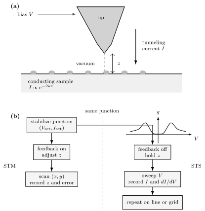
Top: a conducting tip and sample form a voltage-biased vacuum junction whose current is exponentially sensitive to the gap . Bottom: constant-current imaging keeps feedback on and records the required piezo height, whereas point or grid spectroscopy first establishes a setpoint, opens the feedback loop, sweeps , and records and the lock-in estimate of .
The essential instrument contains:
- a conducting sample and a sharpened conducting tip;
- coarse approach and piezoelectric , , and positioning;
- a low-noise bias source and current preamplifier;
- a feedback controller that adjusts to maintain a current setpoint;
- vibration isolation, thermal shielding, electrical filtering, and often ultrahigh vacuum;
- optional cryogenic, magnetic-field, radio-frequency, and optical hardware.
The primary detector variable is current. A topograph is the command required by a feedback law, not a direct height measurement. A conductance spectrum may be obtained by numerical differentiation of or, more commonly, from the first-harmonic response to a small bias modulation. The raw data should retain at least
together with feedback gains, scan direction and speed, lock-in amplitude, frequency, phase and time constant, temperature, field, tip-treatment history, and sample preparation.
Bias and current convention
Section titled “Bias and current convention”This page uses sample bias
with . For a normal-metal tip in the usual elastic-tunneling convention:
- predominantly probes empty sample states between the sample Fermi level and ;
- predominantly probes occupied sample states between and the sample Fermi level.
Laboratories differ in whether positive current denotes conventional charge flow or electron flow. A publication must state both the bias definition and current sign. The words filled-state image and empty-state image are inadequate when tip states, semiconducting band bending, superconducting electrodes, or large biases matter.
Tunneling Current
Section titled “Tunneling Current”Transfer-Hamiltonian expression
Section titled “Transfer-Hamiltonian expression”Bardeen’s weak-coupling construction treats tip and sample as separately equilibrated electrodes and couples their states perturbatively. For tip state and sample state , the matrix element can be evaluated on a surface inside the barrier:
If energy is measured from the sample chemical potential, a useful continuum form of the elastic current is
Here is the tip density of states and is a matrix-element-weighted sample spectrum. The notation deliberately avoids identifying it with the bare sample density of states. Tip orbital symmetry, lateral momentum filtering, barrier shape, surface termination, and the voltage-dependent junction geometry all enter .
The perturbative expression assumes a weak junction. At contact, at very high current, or under strong nonequilibrium drive, multiple scattering, force, heating, and atomic rearrangement invalidate the simple transfer picture.
Exponential distance sensitivity
Section titled “Exponential distance sensitivity”For a locally rectangular barrier of effective height and low bias, a wavefunction decays with
In practical units,
For , retracting the tip by reduces the idealized current by about a factor of eight. This exponential selectivity explains high vertical sensitivity and why vibration, drift, and a second microscopic protrusion on the tip are consequential.
An curve can define an apparent barrier height:
is a junction diagnostic, not automatically the arithmetic mean of independently measured work functions. Image potentials, bias, orbital character, piezo calibration, and mechanical relaxation can change the slope.
Local Spectral Density and the Tersoff–Hamann Limit
Section titled “Local Spectral Density and the Tersoff–Hamann Limit”The local single-particle spectral density is related to the retarded Green function by
For independent particles this reduces to
It is local in real space but summed over whatever momentum, band, spin, and orbital components can tunnel into the tip.
Tersoff and Hamann modeled an -wave tip apex and a weak, low-bias vacuum junction. At low temperature, with a featureless tip spectrum and slowly varying matrix element,
and therefore
This is the central STS approximation. It is powerful precisely because its assumptions are testable. The proportionality can fail or become strongly weighted when:
- the tip density of states varies over the bias window;
- the apex has important - or -orbital character;
- several sample orbitals have different vacuum decay constants;
- the barrier transmission changes rapidly with bias;
- the sample is semiconducting and the tip electric field bends bands;
- the voltage drops outside the intended vacuum barrier;
- the junction becomes inelastic, nonequilibrium, or strongly coupled.
Chen’s derivative rule makes the orbital warning concrete: a nonspherical apex can couple to spatial derivatives of the sample wavefunction rather than simply to its value at . Changing the tip can then reverse contrast or suppress a state without changing the sample.
Thermal and modulation broadening
Section titled “Thermal and modulation broadening”With a normal, featureless tip and bias-independent matrix element, finite temperature gives approximately
The full width at half maximum of is about . At , this thermal width is approximately before electrical noise or lock-in broadening is included.
A lock-in amplifier does not calculate an infinitesimal derivative. It measures a finite-amplitude first harmonic, so the reported conductance is the intrinsic junction response convolved with a kernel fixed by the modulation waveform, amplitude, filter, and phase. Quoting only the base temperature while omitting the bias-modulation amplitude does not specify the energy resolution. The most defensible analysis forward-convolves a spectral model with the thermal, modulation, and electrical response rather than removing broadening by an unstable deconvolution.
Topography Versus Spectroscopy
Section titled “Topography Versus Spectroscopy”Constant-current imaging
Section titled “Constant-current imaging”Let be the geometric surface height and the laboratory piezo coordinate. In a simple low-bias model,
Solving for the recorded piezo coordinate gives
A constant-current topograph therefore combines geometric height, integrated electronic weight, barrier transmission, and tip response. Bias-dependent contrast reversal is often useful evidence of electronic structure, but it is also proof that apparent height is not purely geometric.
The feedback bandwidth must be fast enough to track the intended corrugation and slow enough not to chase current noise. Excessive gain produces ringing; insufficient gain produces tracking error. Trace and retrace disagreement can expose drift, creep, tip changes, or an unstable loop.
Constant-height imaging
Section titled “Constant-height imaging”With feedback disabled, the tip follows a prescribed plane and the current is recorded. Constant-height mode avoids feedback convolution and can be faster, but it is less tolerant of tilt, steps, debris, drift, and piezo nonlinearity. A collision can alter both tip and sample. Constant-height data are meaningful only when the scan plane and safety margin are documented.
Point, line, and grid spectroscopy
Section titled “Point, line, and grid spectroscopy”A common spectroscopy cycle is:
- stabilize the feedback at ;
- wait for the junction and filters to settle;
- open the feedback loop;
- sweep while recording and optionally lock-in ;
- return to the setpoint, close feedback, and move to the next position.
The stabilization step imprints a setpoint effect. In the simple model, the fixed junction height obeys
Consequently, a conductance map scales approximately as
Spatial variation in the integrated denominator can create, suppress, or mix Fourier components. Comparing maps acquired with different setpoints, analyzing the simultaneously acquired current, and forward-modeling the normalization are stronger than assuming the denominator is uniform.
The normalized conductance
can reduce a slowly varying transmission factor and extend dynamic range, especially in semiconductor spectroscopy. It is not model free: the ratio is unstable near zero current or zero bias, requires a declared regularization or smoothing procedure, and can shift or reshape features.
Quasiparticle Interference
Section titled “Quasiparticle Interference”An elastic defect can scatter a quasiparticle from to . Interference between incident and scattered amplitudes modulates the local spectral density. A conductance map
can be drift-corrected, windowed, Fourier transformed, and compared across energy to obtain dispersing features in .
A joint-density-of-states construction,
identifies pairs of high-spectral-weight states separated by . It is a phase-space guide, not a complete QPI theory. In a single-impurity -matrix treatment,
The Green functions carry band, orbital, spin, particle–hole, and coherence-factor structure; the impurity matrix carries the defect potential and scattering channel. Two geometrically allowed vectors can therefore have very different intensities.
A reliable QPI workflow:
- correct drift using the atomic lattice and preserve the transformation metadata;
- inspect the real-space map, defects, step edges, scan-line artifacts, and tip stability;
- compare raw, symmetrized, and differently windowed Fourier transforms;
- separate Bragg peaks, structural superlattices, nondispersive order, and dispersive scattering;
- fit the complete energy-dependent pattern with candidate bands and scattering matrices;
- compare with ARPES or another momentum-resolved probe when possible.
For an isotropic contour, backscattering gives , but that mnemonic is not universal. Multiband, anisotropic, spin-textured, and superconducting systems require vector assignments and coherence factors. Absence of a nominal peak is not by itself proof of topological protection: tip and orbital matrix elements, the impurity population, finite field of view, overlapping features, and signal-to-noise can all hide it. The Edge and Surface States page owns the corresponding topology claim.
Setpoint normalization is especially important in Fourier analysis because the denominator can mix spatial structure from the entire stabilization window into every energy slice. A Fourier peak is an observed modulation; calling it QPI requires dispersion and a scattering model.
Superconducting Gap Imaging
Section titled “Superconducting Gap Imaging”With a normal tip and a simple isotropic superconductor, low-temperature conductance can show suppressed subgap weight and coherence peaks near . Real spectra can instead reflect an anisotropic or nodal gap, several bands, pair breaking, lifetime effects, spatial inhomogeneity, surface states, competing order, and instrumental convolution. BCS Theory gives the ideal density of states and the commonly used Dynes broadening; this page focuses on what a map establishes.
A defensible gap map fits each spectrum to a common forward model:
Here carries parameters such as and , while includes thermal, modulation, and electrical resolution. Fit parameters, bounds, background, rejected pixels, covariance, and residuals should accompany the map. Half the coherence-peak separation is a descriptive energy scale, not a universal estimator of the order parameter.
With a superconducting tip, the conductance contains both electrode spectra. For two fully gapped electrodes, prominent quasiparticle thresholds occur near
not at the sample gap alone. A calibrated superconducting tip can sharpen effective resolution and provide particle–hole mixing information, but tip-gap inhomogeneity and Josephson or nonequilibrium contributions must be modeled.
Useful superconducting imaging modes include:
- maps of fitted gap scale, broadening, zero-bias conductance, and coherence-peak weight;
- field-dependent vortex imaging and vortex-core spectroscopy;
- impurity-bound-state maps and their particle–hole structure;
- energy-resolved QPI with superconducting coherence factors;
- Josephson STM, where pair tunneling probes local phase-coherent response.
A local single-particle gap is not automatically a superconducting order parameter. Temperature and field evolution, phase-sensitive information, vortex response, and bulk thermodynamic or electrodynamic evidence strengthen the assignment. Spatial anticorrelation between two fitted quantities does not establish that one causes the other; setpoint, fit covariance, and shared normalization must be tested.
Atomic Manipulation and Defects
Section titled “Atomic Manipulation and Defects”The tip is an actuator as well as a detector. By reducing the separation, changing the bias, or applying a controlled pulse, an experiment can:
- drag, push, or pull an adsorbate laterally;
- transfer an atom or molecule between tip and sample;
- change a molecular conformation, charge state, or spin state;
- desorb material, create a vacancy, or move a domain wall;
- assemble artificial lattices, corrals, and coupled impurity structures.
Eigler and Schweizer’s low-temperature positioning of individual xenon atoms demonstrated deterministic lateral manipulation. Crommie, Lutz, and Eigler then assembled iron-atom corrals and observed confined surface-state resonances. These experiments establish a workflow, not a universal mechanism: manipulation can be driven by tip–adsorbate forces, electric fields, current-induced excitation, local heating, or chemical transfer, depending on junction parameters.
Before and after images should be acquired with nondestructive settings, and a manipulation threshold should be mapped against current, bias, pulse duration, and approach distance. The current transient and final tip state are part of the evidence. An apparent disappearance may mean transfer to the tip, diffusion outside the field of view, a changed charge state, or changed contrast.
Defects can be studied rather than moved. A point defect may produce a local resonance, Friedel oscillations, a magnetic or superconducting bound state, or a charging feature. Assignment requires comparison among defect species, spatial decay and symmetry, field and temperature response, and a microscopic impurity model. The topographic shape alone rarely identifies the chemical species.
Inelastic STS detects thresholds where tunneling electrons excite a vibration, spin transition, or other local mode. The signal may appear in or as steps in . Heating, vibrational pumping, and competing elastic structure must be excluded. This is a different operator channel from the elastic local spectral density.
Tip-induced perturbations
Section titled “Tip-induced perturbations”The same local electric field and force that enable manipulation can perturb passive spectroscopy:
- semiconductors and low-density systems can exhibit tip-induced band bending;
- small islands and molecules can charge, gate, or undergo Coulomb blockade;
- a magnetic or superconducting tip can exchange-couple or proximity-couple to the sample;
- high current can heat, switch, or damage the surface;
- the apex can pick up atoms and change orbital or spin sensitivity.
Varying tip height and setpoint is therefore a physical control experiment. A feature that shifts with junction resistance may belong to the junction rather than to the unperturbed sample.
Calibration and Reproducible Workflow
Section titled “Calibration and Reproducible Workflow”Before acquisition
Section titled “Before acquisition”- Prepare or cleave the surface under controlled conditions and record elapsed time, pressure, and thermal history.
- Condition the tip on a reference region; verify a single apex using atomic lattice images, step edges, and reproducible spectra.
- Calibrate lateral scale and shear against known lattice vectors, including scanner rotation.
- Calibrate sensitivity and current preamplifier gain; acquire curves over a safe range.
- Verify bias polarity, voltage offset, current sign, lock-in phase, and the energy reference using a known metallic or superconducting spectrum.
- Measure vibration and electrical noise with the feedback loop both closed and open.
During acquisition
Section titled “During acquisition”- save forward and reverse scans and the feedback error channel;
- repeat representative spectra before, during, and after a grid;
- retain topography, current, and conductance acquired under the same setpoint;
- record every change in tip conditioning, scan angle, speed, gain, filter, and setpoint;
- randomize or repeat temperature and field sweeps when drift or aging can mimic a trend;
- avoid processing that overwrites raw coordinates or removes scan-line structure irreversibly.
After acquisition
Section titled “After acquisition”Scanner creep, thermal drift, hysteresis, and nonlinear piezo response can deform a lattice over a long map. Drift correction should use declared fiducials and preserve an uncorrected copy. Plane subtraction, line flattening, Fourier filtering, symmetrization, and registration can all alter long-wavelength or symmetry information. Show enough intermediate data that a reader can distinguish a sample feature from an analysis choice.
Common Artifacts and Failure Modes
Section titled “Common Artifacts and Failure Modes”| Symptom | Plausible cause | Diagnostic |
|---|---|---|
| duplicated atoms or parallel features | double or multiple tip apex | image an isolated defect or step; recondition tip |
| streaks and abrupt contrast changes | tip rearrangement, feedback transient, vibration | compare trace/retrace, error channel, and time order |
| scan-direction-dependent lattice | creep, hysteresis, cross-coupling | rotate scan, reverse direction, calibrate both axes |
| broad or shifted spectral feature | temperature, modulation, voltage offset, tip spectrum | reference spectrum and full resolution convolution |
| spatial contrast changes with setpoint | integrated-density normalization or barrier weighting | repeat several pairs |
| strong low-frequency stripes | line noise, drift, feedback gain, flattening | inspect raw lines, noise spectrum, and scan-speed scaling |
| feature moves with junction resistance | band bending, charging, heating, force | vary tip height at fixed location and model electrostatics |
| Fourier peak appears after symmetrization | processing or finite-window artifact | show unsymmetrized maps and alternate windows |
| gap map follows topography | setpoint, tip change, or fit covariance | compare raw spectra, residuals, and independent setpoints |
| atom changes identity after a pulse | tip pickup or charge-state contrast | reimage reference surface and characterize the apex |
An uncertainty budget should separate at least:
- coordinate uncertainty: scanner calibration, drift, creep, and registration;
- energy uncertainty: voltage calibration, offset, thermal width, modulation kernel, and noise;
- amplitude uncertainty: preamplifier gain, lock-in phase, feedback state, and normalization;
- junction uncertainty: tip spectrum and orbital character, barrier, setpoint, and voltage division;
- sample uncertainty: surface termination, contamination, domains, aging, and preparation history;
- model uncertainty: background, fit family, impurity potential, band assignment, and parameter covariance.
Repeated pixels in one map are not independent preparations. Reproducibility across tips, cleaves, samples, and acquisition sequences is stronger evidence than a small fit error on one large grid.
Common Mistakes
Section titled “Common Mistakes”- Calling a topograph atomic positions. It is a constant-current isosurface shaped by geometry and integrated electronic weight.
- Writing without assumptions. Temperature, tip states, matrix elements, barrier transmission, and setpoint enter.
- Inferring bias polarity from a software label. State the electrical convention and verify it experimentally.
- Treating lock-in output as an exact derivative. Finite modulation is a convolution and contributes to energy resolution.
- Comparing maps with different setpoints as though only energy changed. Junction height and normalization changed too.
- Assigning every Fourier peak to QPI. Bragg peaks, order, drift, windows, and scan-line artifacts can be nondispersive.
- Reading a superconducting order parameter directly from peak spacing. Electrode convolution, anisotropy, broadening, and competing gaps intervene.
- Assuming an atomically sharp tip has a known orbital. The apex is part of the measurement operator and can change mid-scan.
- Using symmetry averaging as evidence of symmetry. Symmetrization imposes what it is supposed to test.
- Equating local surface evidence with a bulk phase. Combine STM/STS with bulk-sensitive and phase-sensitive measurements.
Connections
Section titled “Connections”- Unconventional Superconductivity places local gap, node, and sign-sensitive clues into a crystal-symmetry evidence ledger; this page retains the tip, surface, tunneling-matrix, feedback, and convolution forward model.
- How Quantum Matter Is Measured supplies the general record-to-claim and uncertainty framework.
- Spectral Functions gives the canonical many-body meaning of local addition and removal weight.
- Angle-Resolved Photoemission Spectroscopy provides complementary momentum-resolved, spatially averaged surface spectroscopy.
- Charge and Spin Density Waves distinguishes static order from dispersive interference and sets the multi-probe standard for density-wave claims.
- Weyl and Dirac Semimetals uses surface spectroscopy and QPI as part of a broader bulk–surface evidence package.
- BCS Theory owns ideal superconducting spectra, coherence factors, and the distinction between fit broadening and microscopic lifetime.
- Superconducting Proximity Effect predicts spatial minigaps, anomalous-amplitude profiles, and inverse suppression in inhomogeneous superconductors, while this page retains tip, setpoint, matrix-element, convolution, and surface-preparation effects.
- Vortex Matter, Pinning, and Flux Flow uses calibrated vortex positions and their field, temperature, and history dependence to test collective order and pinning, while this page retains tunneling setpoints, spectral convolution, and local core imaging.
References
Section titled “References”- J. Bardeen, “Tunnelling from a Many-Particle Point of View”, Physical Review Letters 6, 57–59 (1961).
- G. Binnig, H. Rohrer, Ch. Gerber, and E. Weibel, “Surface Studies by Scanning Tunneling Microscopy”, Physical Review Letters 49, 57–61 (1982).
- J. Tersoff and D. R. Hamann, “Theory and Application for the Scanning Tunneling Microscope”, Physical Review Letters 50, 1998–2001 (1983).
- J. Tersoff and D. R. Hamann, “Theory of the Scanning Tunneling Microscope”, Physical Review B 31, 805–813 (1985).
- C. J. Chen, “Tunneling Matrix Elements in Three-Dimensional Space: The Derivative Rule and the Sum Rule”, Physical Review B 42, 8841–8857 (1990).
- R. M. Feenstra, “Tunneling Spectroscopy of the (110) Surface of Direct-Gap III–V Semiconductors”, Physical Review B 50, 4561–4570 (1994).
- J. E. Hoffman et al., “Imaging Quasiparticle Interference in BiSrCaCuO”, Science 297, 1148–1151 (2002).
- Q.-H. Wang and D.-H. Lee, “Quasiparticle Scattering Interference in High-Temperature Superconductors”, Physical Review B 67, 020511(R) (2003).
- Ø. Fischer, M. Kugler, I. Maggio-Aprile, C. Berthod, and C. Renner, “Scanning Tunneling Spectroscopy of High-Temperature Superconductors”, Reviews of Modern Physics 79, 353–419 (2007).
- S. H. Pan et al., “Microscopic Electronic Inhomogeneity in the High- Superconductor BiSrCaCuO”, Nature 413, 282–285 (2001).
- Y. Hasegawa and P. Avouris, “Direct Observation of Standing Wave Formation at Surface Steps Using Scanning Tunneling Spectroscopy”, Physical Review Letters 71, 1071–1074 (1993).
- M. F. Crommie, C. P. Lutz, and D. M. Eigler, “Imaging Standing Waves in a Two-Dimensional Electron Gas”, Nature 363, 524–527 (1993).
- D. M. Eigler and E. K. Schweizer, “Positioning Single Atoms with a Scanning Tunnelling Microscope”, Nature 344, 524–526 (1990).
- M. F. Crommie, C. P. Lutz, and D. M. Eigler, “Confinement of Electrons to Quantum Corrals on a Metal Surface”, Science 262, 218–220 (1993).
- B. C. Stipe, M. A. Rezaei, and W. Ho, “Single-Molecule Vibrational Spectroscopy and Microscopy”, Science 280, 1732–1735 (1998).
- Joint Committee for Guides in Metrology, Evaluation of Measurement Data — Guide to the Expression of Uncertainty in Measurement, JCGM 100:2008.
Exercises
Section titled “Exercises”Exercise 1: Current–distance sensitivity
Section titled “Exercise 1: Current–distance sensitivity”Take an effective barrier height . Estimate and the current ratio in the rectangular-barrier approximation.
Solution
The inverse decay length is
Therefore
A one-ångström retraction lowers the current by a factor of about . The exact factor is junction dependent because and the orbital matrix element are effective quantities.
Exercise 2: Electronic corrugation in a topograph
Section titled “Exercise 2: Electronic corrugation in a topograph”At fixed geometric height, suppose the integrated spectral weight doubles between two sites while . What apparent height difference is required to keep the current constant?
Solution
At constant current,
Thus
The feedback retracts the tip over the electronically brighter site. The recorded corrugation is electronic even though the geometric surface is flat.
Exercise 3: Thermal energy resolution
Section titled “Exercise 3: Thermal energy resolution”Estimate the full width at half maximum of the thermal kernel at . Use .
Solution
The width is
This is only the thermal contribution. Bias modulation, voltage noise, filtering, and the tip spectrum broaden the measured feature further.
Exercise 4: Bias polarity
Section titled “Exercise 4: Bias polarity”Under this page’s convention, . Which side of the sample spectrum is emphasized at with a normal featureless tip, and why?
Solution
Positive sample bias predominantly allows occupied tip states to tunnel into empty sample states. At low temperature, the main window extends from to approximately . The measurement therefore emphasizes the sample’s unoccupied side.
This answer depends on the declared voltage convention. A software channel called “bias” is not sufficient evidence of polarity.
Exercise 5: A QPI wavelength
Section titled “Exercise 5: A QPI wavelength”An approximately circular constant-energy contour has radius . If a visible modulation is assigned to backscattering, estimate its wavevector magnitude and real-space wavelength.
Solution
For ideal backscattering,
The corresponding real-space wavelength is
The numerical conversion does not validate the assignment. Orbital and spin overlap, the impurity matrix, alternative interband vectors, setpoint mixing, and the observed energy dispersion must also agree.
Exercise 6: Superconducting-tip threshold
Section titled “Exercise 6: Superconducting-tip threshold”A fully gapped sample has and a calibrated superconducting tip has . Where should the simplest quasiparticle thresholds occur at low temperature?
Solution
For two fully gapped electrodes, quasiparticle tunneling turns on strongly near the sum of the gaps:
The corresponding bias magnitudes are approximately . Reading the observed threshold as would overestimate the sample gap. A quantitative fit must still include temperature, broadening, both electrode spectra, and any Josephson contribution near zero bias.